Ac To Dc
Found 8 free book(s)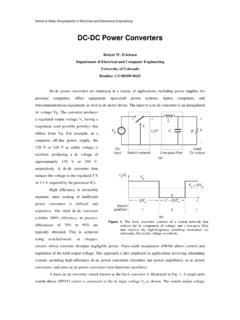
DC-DC Power Converters
ecee.colorado.educurrent, including high-efficiency dc-ac power converters (inverters and power amplifiers), ac-ac power converters, and some ac-dc power converters (low-harmonic rectifiers). A basic dc-dc converter circuit known as the buck converter is illustrated in Fig. 1. A single-pole double-throw (SPDT) switch is connected to the dc input voltage V g as ...

AC 70/7460-1M Obstruction Marking and Lighting
www.faa.govAC 70/7460-1L, change 2, Obstruction Marking and Lighting, dated August 2018 is cancelled by this version.
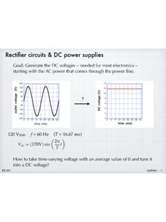
Rectifier circuits & DC power supplies
tuttle.merc.iastate.eduNov 01, 2015 · transformer peak rectifier regulator DC load 120 V RMS transformer : reduces AC amplitude to something safe and manageable. V peak from the transformer will be a few volts bigger than the desired DC voltage. peak rectifier : breaks up the AC waveform and produces a V DC ≈ V peak . regulator : Refines the output of the rectifier. (optional ...
Spartan-3E FPGA Family Data Sheet (DS312)
www.xilinx.comDC and Switching Characteristics DS312 (v4.2) December 14, 2018 † DC Electrical Characteristics † Absolute Maximum Ratings † Supply Voltage Specifications † Recommended Operating Conditions † DC Characteristics † Switching Characteristics † I/O Timing † SLICE Timing g n i m i TM C†D † Block RAM Timing † Multiplier Timing

GlobalLFSeriesPureSineWaveInverterCharger User’sManual
www.aimscorp.net(2) DC voltage on inverter (7) Output frequency (3) Load when inverting (8) Bypass/ inverter mode (4) Low/high voltage, over temp, overload (9) Battery state of charge graph (5) Fault condition NOTE: The battery icon is just an image and does not …
Virtex-7 T and XT FPGAs Data Sheet: DC and AC Switching ...
www.xilinx.comVirtex-7 T and XT FPGAs Data Sheet: DC and AC Switching Characteristics DS183 (v1.29) March 23, 2021 www.xilinx.com Product Specification 4 IRPU Pad pull-up (when selected) @ VIN =0V V, CCO = 3.3V 90 – 330 µA Pad pull-up (when selected) @ VIN =0V V, CCO = 2.5V 68 – 250 µA Pad pull-up (when selected) @ VIN =0V V, CCO = 1.8V 34 – 220 µA Pad pull-up (when …
EE101: RLC Circuits (with DC sources)
www.ee.iitb.ac.inSeries RLC circuit i R L C VR VC VL V0 KVL: V R + V L + V C = V0)i R + L di dt + 1 C Z i dt = V0 Di erentiating w. r. t. t, we get, R di dt + L d2i dt2 1 C i = 0. i.e., d2i dt2 R L di dt + 1 LC i = 0, a second-order ODE with constant coe cients.

E1.1 Circuit Analysis Problem Sheet 1 (Lectures 1 & 2)
www.ee.ic.ac.ukVer 2427 E1.1 Analysis of Circuits (2014) E1.1 Circuit Analysis Problem Sheet 1 - Solutions 1. Circuit (a) is a parallel circuit: there are only two nodes and all four components are connected