
Chapter 23: Wafer Level Packaging
through-hole packaging to the advanced systems we have today using 10nm-technology-node manufacturing and a wide range of advanced packaging platforms, addressing single- and multi-die packaging. Major technology advances in semiconductors were mainly driven by Moore’s Law and scaling the technology
Download Chapter 23: Wafer Level Packaging

Information
Domain:
Source:
Link to this page:
Documents from same domain

Chapter 1: HIR Overview and Executive Summary
eps.ieee.orginnovation in design and process technologies continue the drive to advanced nodes, Moore’s-Law economics and performance are evidently plateauing. Shown below are two graphs presented by John Hennessy at the ERI Conference in July 2018 [5]. The graph to the left shows forty years of DRAM capacity and the slowing down of

Chapter 9: Integrated Photonics
eps.ieee.orgelectronics, photonics and plasmonics will be required to address these substantial new challenges in order to meet the expanding requirement for higher performance, higher reliability, increased security, lower latency and continued decrease in cost per function. The packaging of photonic integrated circuits (PICs) will face the same challenges

Chapter 23: Wafer-Level Packaging (WLP) - IEEE
eps.ieee.orgWafer level packaging is where a die is packaged while still in wafer form, either singly or combined with additional dies or other components such as discrete passive devices, or …
Related documents
Semiconductor Manufacturing Equipment - USITC
www.usitc.gov4 For more information on the semiconductor industry, please refer to Box 1. 3 INTRODUCTION Semiconductor manufacturing equipment (SME) is used in perhaps the most complex and advanced manufacturing process in the world, the production of semiconductor devices.1 Semiconductors, such as microprocessors and memory devices, are used in a wide variety
Semiconductors: U.S. Industry, Global Competition, and ...
sgp.fas.orgSemiconductors are also a top U.S. export. Semiconductor design and manufacturing is a global enterprise with materials, design, fabrication, assembly, testing, and packaging operating across national borders. Six U.S.-headquartered or foreign-owned semiconductor companies currently operate 20 fabrication facilities, or fabs, in the United States.

NC7WZ07 SIP6 UDFN6 - ON Semiconductor
www.onsemi.comON Semiconductor reserves the right to make changes without further notice to any products herein. ON Semiconductor makes no warranty, representation or guarantee regarding the suitability of its products for any particular purpose, nor does ON Semiconductor assume any liability arising out of the application or use of any product or circuit ...

Semiconductors and Intel
www.intel.comPackaging: protect, connect and re-architect New packaging technologies allow the combination of myriad die into “systems in packages,” enabling more design and performance flexibility —leading to entirely new kinds of chips, like the powerful Ponte Vecchio GPU. Intel is a world leader in advanced packaging development and manufacturing.

January 25, 2022 H.R. 4521, The America COMPETES Act of 2022
www.speaker.govsemiconductor manufacturing R&D under the Manufacturing USA Program, and establish an advanced packaging R&D program. • This bill provides substantial financial assistance to incentivize investment in facilities and equipment for semiconductor fabrication, assembly, testing, advanced packaging, and research and development.
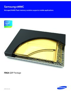
Samsung eMMC
semiconductor.samsung.comwith advanced security and reliability features. Increase storage capabilities for diverse applications Advanced mobile devices and handsets can use Samsung eMMC to expand computing power and content storage. Enhanced storage solutions for mobile devices that provide high-density solid state memory can be integrated into system designs.
MULTINATIONAL SEMICONDUCTOR COMPANY ORDERS …
www.semiconductorpackagingnews.comMar 23, 2022 · of ownership that enables growth of the advanced packaging market. According to Yole Développement, the global advanced packaging market is projected to grow at an 8 percent compound annual growth rate and reach $48.2 billion USD by 2026. About Veeco Veeco (NASDAQ: VECO) is an innovative manufacturer of semiconductor process equipment. Our

Press Release - semiconductorpackagingnews.com
www.semiconductorpackagingnews.comsheets of self-adhesive synthetic graphite on top of critical semiconductor devices in order to conduct away waste heat from small areas. Aerospace, defense and space applications require more precision, repeatability and area of coverage. To address this, Teledyne Labtech has developed a method of embedding thin layers of synthetic