
Innovus Implementation System
high-density designs at advanced and established process nodes, the Innovus Implementation System delivers a typical 10%-20% PPA advantage along with an up to 10X TAT gain. Providing the industry’s first massively parallel solution, the Innovus Implementation System can effectively handle blocks as large as 5-10 million instances or more.
Download Innovus Implementation System

Information
Domain:
Source:
Link to this page:
Documents from same domain
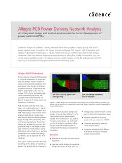
Allegro PCB Power Delivery Network Analysis - Cadence
www.cadence.comAllegro PCB Power Delivery Network Analysis Cadence is transforming the global electronics industry through a vision called EDA360. With an application-driven approach to design, our software, hardware, IP, and services help
Routing DDR4 Interfaces Quickly and Efficiently
www.cadence.comDesign rules above are for reference only and should be treated as such—only tried and true way to determine interface design rules is with pre- /post-route simulations DDR4 Design Rules

Holistic FMEDA-Driven Safety Design and Verification for ...
www.cadence.comThe integration of these ... In recent years, safety design and verification for digital circuits have made great progress. However, more than 80% of field failures are due to the analog or mixed-signal portion of products [4]. Hence the safety methodology must be enhanced to ... deployed later in the SoC design process.

Chiplets and Heterogeneous Packaging Are Changing System ...
www.cadence.comChiplets and Heterogeneous Packaging Are Changing System Design and Analysis www.cadence.com 2 Introduction The semiconductor packaging industry is now poised to take on a larger, more significant role in electronic product design of the future. To meet the market demand for these heterogenous, chiplet-based architectures (Figure 1), new system ...

Master Learning Maps - cadence.com
www.cadence.comBehavioral Modeling with VHDL-AMS Command-Line Based Mixed-Signal Simulations w/ Xcelium r Use Model r Circuit Design, Simulation, Modeling and RF Design Custom IC, Analog and RF Design Learning MapLearning Map Digital Design and Signoff Mixed-Signal Simulations using Spectre AMS Designer Analog Modeling with Verilog-A Behavioral Modeling with ...

Keeping Things Quiet: A New Methodology for Dynamic ...
www.cadence.comVirtuoso AMS Designer Mixed-signal verification with Incisive® solution Virtuoso® Analog Design Environment (ADE) Simulation environment Liberate™ Solution Characterization Voltus™-FI Solution EMIR

DO-254 Explained
www.cadence.comstandard used on commercial electronics that go into aircraft. (Conceptually speaking, this standard applies to all electronics in anything that flies or could crash and pose a hazard to the public.) DO-254 Explained By Cadence This white paper, the first in a series of DO-254-related white papers, will explore the high-level concepts
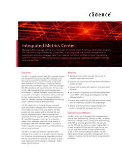
Integrated Metrics Center Technical Brief
www.cadence.comcoverage—block, expression, toggle, and finite state machine (FSM)—as well as assertion and functional coverage. An activity center consists of a coverage metrics window, a source code window, an attributes window, and often, depending on the type of metric, an additional deep-dive analysis window. The
Related documents

HP BladeSystem c-Class enclosure
h10032.www1.hp.comsupport modular server, interconnect, and storage components today and throughout the next several years. The enclosure is10U high and holds up to 16 server and/or storage blades plus optional redundant network and storage interconnect modules. It includes a …

Flip Chip BGA (FCBGA)
c44f5d406df450f4a66b-1b94a87d576253d9446df0a9ca62e142.ssl.cf2.rackcdn.comsingle unit laminate or ceramic substrates. Utilizing multiple high-density routing layers, laser drilled blind, buried and stacked vias, and ultra-fine line/space metallization, FCBGA substrates have the highest routing density available. By combining flip chip interconnect with ultra-advanced substrate technology, FCBGA packages can be

DELL EMC POWERSWITCH S4048-ON SWITCH
i.dell.com• High-density 10GbE ToR server access in high-performance data center environments When running the Dell EMC Networking OS9, Active Fabric™ implementation for large deployments in conjunction with the Dell EMC Z-Series, creating a flat, two-tier, nonblocking 10/40GbE data

FIREFLY - Samtec
suddendocs.samtec.comOn-package interconnect enables 56 Gbps PAM4 performance, eliminates distortion through the BGA region and improves density. MT Low insertion force connectors for high-density cabling and backplane applications MPO (MTP®) High-density connectors for panel applications and minimal keep-out areas on the board MXC® High-density connectors

Low- κ Dielectrics - Stanford University
web.stanford.edu5 ta nfo rdU ivesy 9 EE311/ Low-k Dielectrics araswat •Reduce polarization strength and density. •Reduce Si-O density: SiO 2 (k=4) •Incorporate F: SiOF(k =3.7) •Incorporate CH3-: SiOC(H) (k=2.8) •Use low polarization polymer: (Ref.: K.J. Miller et al., Macromolecules, 23, 3855 (1990).) Dielectric Constant Reduction Methods ta nfo rdU ivesy 10 EE311/ Low-k Dielectrics

Your Source for Interconnect Products
www.mouser.comHD designates High Density 38999 Series III insert patterns which use size 23 contacts only. Not rated over 175°C. * Hermetic inserts - solder termination standard. (Contact Amphenol Aerospace for optional PCB or eyelet termination). ** Two size 16 contacts dedicated to fiber optics. See the Fiber Optic section for more information.

Power MOSFET Basics: Understanding MOSFET Characteristics ...
www.vishay.coma density of 178 million cells/inch2. This is a slice through the actual ultra-high-density cell wafer in an area that demonstrates the high-density cell scaling. To achieve such a cell figure, the focus has been placed on both the lateral and vertical cell scaling, optimizing not only the rDS(on) but also the gate characteristics.