
電路佈線(Layout) - 國立中興大學
g.跳出Property Editor 視窗,以拖曳方式選取各元件的PCB Footprint 的欄位後,叫出快 顯選單選取Edit(圖28)。 圖28 圖29 圖30 h.跳出Edit Property Values 後即可根據二極體的規格(圖29)設定Footprint(圖30,可自 Library Manager 處複製後在此貼上以免鍵錯)。 Footprint)
Download 電路佈線(Layout) - 國立中興大學

Information
Domain:
Source:
Link to this page:
Documents from same domain
BJT륱걹쏨 - ezphysics.nchu.edu.tw
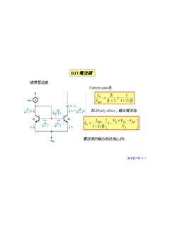
ezphysics.nchu.edu.tw삳ꗎ륱ꑬ뻇10-15 BJT륱걹쏨 볐럇륱걹쏨 Current gain결 b b b 1 2/ 1 REF 2 + I I O ꕛꑗEarly effectꅁ뿩ꕘ륱걹결 + − + + ≈ A O EE BE

Exercise 5 Razavi Prob. 3.32 4. Razavi Prob. 3
ezphysics.nchu.edu.twExercise 5 . 1. Razavi Prob. 3.32 2. Razavi Prob. 3.34 3. Razavi Prob. 3.37 . Author: YWSuen Created Date: 4/7/2017 9:26:48 AM
Related documents

Getting Started in KiCad
docs.kicad.orgKiCad has separate windows for drawing the schematic ("Schematic Editor"), laying out the board ("PCB. Editor"), and editing symbols and footprints ("Symbol Editor" and "Footprint Editor"). KiCad comes with a. large library of high quality, user contributed symbols and footprints, but it is also simple to create new

Fusion 360 Electronics Migration Guide for EAGLE Users
assets.library.io2D PCB Editor 18 DESIGN menu 18 DOCUMENT menu 19 RULES ERC/DRC menu 20 MANUFACTURING menu 20 AUTOMATION menu 21 LIBRARY menu 21 Command shortcuts 21 9 User Language Programs and Scripts in Fusion 360 Electronics 22 eagle.scr 24 10 Use Your Eagle Libraries and Manage Libraries in Fusion 360 24 Library Manager 24 In Design 25 In …