LP2985-N Micropower 150-mA Low-Noise Ultra-Low …
ON/OFF C OUT 2.2 µ F LP2985 ON/OFF C BYPASS 0.01 µ F GND IN BYPASS V IN OUT V OUT C IN 1 µ F Product Folder Sample & Buy Technical Documents Tools & …
Download LP2985-N Micropower 150-mA Low-Noise Ultra-Low …
Information
Domain:
Source:
Link to this page:
Documents from same domain

LM136-2.5,LM236-2.5,LM336-2 - TI.com
www.ti.comLM136-2.5/LM236-2.5/LM336-2.5V Reference Diode General Description The LM136-2.5/LM236-2.5 and LM336-2.5 integrated cir-cuits are …

SimpleLink™ CC3120, CC3220 Wi-Fi ... - Texas …
www.ti.comUser User x x x x x x x x x x x x x x x x x x x x Application Servers Vendor IoT Devices Internet Introduction www.ti.com 4 SWRA509A–February 2017–Revised March 2017 Submit Documentation Feedback

www.ti.com SNVS749F - Texas Instruments
www.ti.comLM136-2.5-N SNVS749F – MAY 1998– REVISED APRIL 2013 www.ti.com Typical Performance Characteristics (continued) Temperature Drift Figure 13. …

MSP430x2xx Family User's Guide (Rev. J) - TI.com
www.ti.comMSP430x2xx Family User's Guide Literature Number: SLAU144J December 2004– Revised July 2013

1.8-V Micropower CMOS Operational Amplifier …
www.ti.com5 OPA2333-HT www.ti.com SBOS483I –JULY 2009–REVISED MAY 2015 Product Folder Links: OPA2333-HT Copyright © 2009–2015, Texas Instruments Incorporated Submit Documentation Feedback

LMC6482 CMOS Dual Rail-To-Rail Input and Output ...
www.ti.comLMC6482 www.ti.com SNOS674E –NOVEMBER 1997–REVISED APRIL 2015 5 Pin Configuration and Functions D, DGK and P Packages 8-Pin SOIC, VSSOP and PDIP (Top View) Pin Functions PIN TYPE DESCRIPTION NO.

OPAx354 250-MHz, Rail-to-Rail I/O, CMOS …
www.ti.comOPA354 IN +IN V OUT V+ V Product Folder Order Now Technical Documents Tools & Software Support & Community Reference Design An IMPORTANT NOTICE at the end of this data sheet addresses availability, warranty, changes, use …

Analog linearization of resistance temperature …
www.ti.com21 Analog Applications Journal Texas Instruments Incorporated 4Q 2011 www.ti.com/aaj High-Performance Analog Products …

TMS320C28x DSP/BIOS 5.x Application …
www.ti.comSPRU625L—August 2012 API Functional Overview 9 Submit Documentation Feedback www.ti.com Naming Conventions 1.2 Naming Conventions The format for a DSP/BIOS operation name is a 3- or 4-letter prefix for the module that contains the

WL18x7MOD WiLink™ 8 Dual-Band Industrial …
www.ti.comProduct Folder Order Now Technical Documents Tools & Software Support & Community Reference Design An IMPORTANT NOTICE at the end of this data sheet addresses availability, warranty, changes, use in safety-critical applications,
Related documents

Advanced Heating & Hot Water Systems
www.htproducts.comAdvanced Heating & Hot Water Systems 316L Stainless Steel Indirects & Storage Tanks NO ANODE RODS NEEDED RESISTS SCALE BUILD UP LIGHT WEIGHT The Best Selling Indirects In …
LTC6268-10/LTC6269-10 – 4GHz Ultra-Low Bias Current FET ...
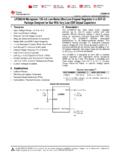
www.analog.comLTC6268-10/LTC 6269-10 1 626810f For more information www.linear.com/LTC6268-10 TYPICAL APPLICATION FEATURES DESCRIPTION 4GHz Ultra-Low Bias Current FET Input Op Amp
LTZ1000/LTZ1000A - Ultra Precision Reference
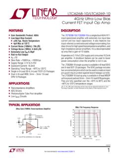
www.analog.comL11 1 1 For more information www.linear.com/LTZ1000 Typical applicaTion FeaTures applicaTions DescripTion Ultra Precision Reference The LTZ1000 and LTZ1000A are ultra ...
LDO Regulator - Ultra-Low Noise, High PSRR, RF and Analog ...
www.onsemi.comNCP163 www.onsemi.com 4 ELECTRICAL CHARACTERISTICS −40°C ≤ TJ ≤ 125°C; VIN = VOUT(NOM) + 1 V; IOUT = 1 mA, CIN = COUT = 1 F, unless otherwise noted. VEN = 1.2 V. Typical values are at TJ = +25°C (Note 4). Parameter Test Conditions Symbol Min Typ Max Unit Output Voltage Noise f = 10 Hz to 100 kHz IOUT = 1 mA IOUT = 250 mA VN 8.0
NCP718 - Low Dropout Regulator, Wide Input Voltage, Low Iq ...
www.onsemi.comNCP718 www.onsemi.com 3 Table 4. ELECTRICAL CHARACTERISTICS -40°C ≤ TJ ≤ 125°C; VIN = 2.5 V or (VOUT + 1.0 V), whatever is greater; IOUT = 1 mA, CIN = COUT = 1 F, unless otherwise noted. Typical values are at TJ = +25°C. (Note 3) Parameter Test Conditions Symbol Min Typ Max Unit Operating Input Voltage VIN 2.5 24 V Output Voltage Accuracy
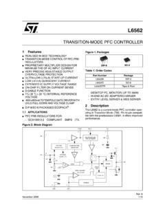
Transition-mode PFC controller
www.st.com1/16 l6562 november 2005 1features realised in bcd technology transition-mode control of pfc pre- regulators proprietary multiplier design for minimum thd of ac input current very precise adjustable output overvoltage protection ultra-low ( ≤70µa) start-up current low (≤4 ma) quiescent current extended ic supply voltage range on-chip filter on current sense
K i n t e x U l t r a S c a l e + F P G A s D a t a S h e ...
www.xilinx.comS u m m a r y The Xilinx® Kintex® UltraScale+™ FPGAs are available in -3, -2, -1 speed grades, with -3E devices having the highest performance. The -2LE and -1LI devices can operate at a VCCINT voltage at 0.85V or 0.72V and provide lower maximum static power. When operated at VCCINT = 0.85V, using -2LE and -1LI devices, the speed specification for the L devices is the same as the -2I or ...