Transcription of Transmission Line Basics - ntuemc.tw
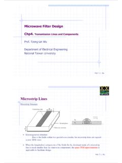
1 1 Transmission line Basics Prof. Tzong-Lin Wu NTUEE 2 Outlines Transmission Lines in Planar structure. Key Parameters for Transmission Lines. Transmission line Equations. Analysis Approach for Z0 and Td Intuitive concept to determine Z0 and Td Loss of Transmission Lines Example: Rambus and RIMM Module design 3 Transmission Lines in Planar structure Homogeneous Inhomogeneous Coaxial Cable Stripline Microstrip line Embedded Microstrip line 4 Key Parameters for Transmission Lines of V / I : Characteristic Impedance Z0 of Signal: Effective dielectric constant e : Conductor loss ac Dielectric loss ad Z0 LC1 LCce0 Vp1Td1 VCpTCdLossless case 5 Transmission line Equations Quasi-TEM assumption 6 Transmission line Equations RGLC0000 resistance per unit length(Ohm/cm)conductance per unit length (mOhm/cm)inductance per unit length (H/cm)capacitance per unit length (F/cm)dVdzRjwLIdIdzGjwCV ()()0000 KVL : KCL.
2 Solve 2nd order for V and I 7 Transmission line Equations VVeVeIZVeVeIIrzrzrzrz 10()Two wave components with amplitudes V+ and V- traveling in the direction of +z and -z Where propagation constant and characteristic impedance are rRjwLGjwCj ()()0000a ZVIVIRjwLGjwC00000 8 Transmission line Equations a a 220020000002 RGLCRCGL()a and can be expressed in terms of (RLGC0000,,,)The actual voltage and current on Transmission line : VztVeeVeeeIztZVeeVeeezjzzjzjwtzjzzjzjwt( ,)Re[()](,)Re[()] a a a a 109 Analysis approach for Z0 and Td (Wires in air) C = ? (by Q=C V) L = ? (by =L I) 10 Analysis approach for Z0 and Td (Wires in air): Ampere s Law for H field cIIH(r)=2rd 210012 IIR 2) ln() (in Wb)2 r2 RReTSr RB d sdr 11 Analysis approach for Z0 and Td (Wires in air): Ampere s Law for H field 021ln( )2/eeIRRLI 12 The per-unit-length Parameters (E): Gauss s Law 1200TC0201 1) from gauss law 1m 2 2) V= E2R ln2 RTtotalSTSRrRDE d sQqEdsqrqddrrq 13 The per-unit-length Parameters (E) 201ln( )2/qRVRC Q V 14 (note homogeneous medium) Inductance rw1 rw2 S II e 00( , ) 0w20w1w1w20w2w1w1 w2w1w220w1 w2L=IwhereIs-rIs-rln()+ln()2r2rI(s-r )(s-r ) =ln()2r rassume sr , rL=ln()2r reees c.
3 For example Determine the of the two-wire Capacitance 0002w1 w2w2w10w10w2w2w10w1 w22w1w20w1 w202w1 w21) 2 ln ()rrs-rs-rqq2) V=ln()+ln()2r2r(s-r )(s-r )q =ln()2r rq ln() if sr , r2r r2q C= Vln ()rrecCsss the same with 1) approach rw1 rw2 S + + + + + - - - - - - V q C/m -q C/m 16 The per-unit-length Parameters Homogeneous structure TEM wave structure is like the DC (static) field structure LGLC So, if you can derive how to get the L, G and C can be obtained by the above two relations. 17 The per-unit-length Parameters (Above GND ) 2C L/2 Why? 18 d. How to determine L,C for microstrip- line . 00, 11, 00 01) This is inhomogeneous ) Nunerical method should be used to solve the C of this structure, such as Finite element, Finite ) But can be obtained by eeC 000010 where C is the capacitance when medium is replaced by 19 Analysis approach for Z0 and Td (Strip line ) Approximate electrostatic solution 1.
4 2. The fields in TEM mode must satisfy Laplace equation where is the electric potentialThe boundary conditions are at at txyxyxaxyyb200200 (,)(,)/(,),x bya/2-a/220 11cossinh for 0/ 2( , )cossinh() for / 2nnoddnnoddn xn yAybaaxyn xnBb ybybaa Analysis approach for Z0 and Td 3. Since the center conductor will contain the surface charge, so 4. The unknowns An and Bn can be solved by two known conditions: The potential at must continuousThe surface charge distribution for the strip: for for ybxWxWs RSTRS|T|///21202 Why? 21 Analysis approach for Z0 and Td 5. VExydyxyyxydyQxdxWCmybbsww RS||T||zzz (,)(,)/(,)()(/)////00020222 6. CQVWanWanbannbaZvCcCrnoddpr 222212010sin(/)sinh(/)()cosh(/) 7. Answers!! Tcdr /22 Analysis approach for Z0 and Td (Microstrip line ) 1. The fields in Quasi-TEM mode must satisfy Laplace equation where is the electric potentialThe boundary conditions are at at txyxyxaxyy200200 (,)(,)/(,),2.
5 X PECPECa/2-a/2yWd23 (,)cossinhcos/xyAnxanyaydBnxaedynnoddnny anodd RS||T|| for for 0113. Since the center conductor will contain the surface charge, so 4. The unknowns An and Bn can be solved by two known conditions and the orthogonality of cos function : The potential at must continuousThe surface charge distribution for the strip: for for ydxWxWs RSTRS|T| 1202//Analysis approach for Z0 and Td (Microstrip line ) 24 5. VExydyxyyxydyAndaQxdxWCmybnnoddbsww RS||T||z zz (,)(,)/(,)sinh()(/)////000210222 6. CQVWanWandanWndandarnodd 422201sin(/)sinh(/)()[sinh(/)cosh(/)] Analysis approach for Z0 and Td (Microstrip line ) 25 Analysis approach for Z0 and Td (Microstrip line ) To find the effective dielectric constant we consider two cases of capacitance1. C=capacitance per unit length of the microstrip line with the dielectric substrate C=capacitance per unit length of the microstrip line with the dielectric substrate er0r.
6 1217. eCC08. ZvCcCpe01 Tcde /26 Tables for Z0 and Td (Microstrip line ) Z0 20 28 40 50 75 90 100 CpF/mm)0( LnH/mm)0( eff Tps/mm)0(() Fr4 : dielectric constant = Frequency: 1 GHz 27 Z0 20 28 40 50 75 90 100 CpF/mm)0( LnH/mm)0( eff Tps/mm)0(() Tables for Z0 and Td (Strip line ) Fr4 : dielectric constant = Frequency: 1 GHz 28 Analysis approach for Z0 and Td (EDA/Simulation Tool) Touch Stone (HP ADS) Office shop on Web: ( ) ( or ) 29 Concept Test for Planar Transmission Lines Please compare their Z0 and Vp (a) (b) 30 (a) (b) (c) 31 (a) (b) (c) 32 33 ZRjwLjwCLCjxrRjwLjwCj000000120001 ()()()/a Typically, dielectric loss is quite small -> G0 = 0. Thus where xRwL 00 Lossless case : x = 0 Near Lossless: x << 1 Highly Lossy: x >> 1 Loss of Transmission Lines wRL 00 Highly Lossy wNear Lossless w34 Loss of Transmission Lines a LNMOQP FHGIKJ RLCLCxZLCjRwLLCjwCCTRTLC0000020000000000 002181212// where Time delay For Near Lossless case: For Lossless case: a 000000000 LCZLCTLCTime delay 35 Loss of Transmission Lines For highly loss case: (RC Transmission line ) a wRCxwRCxZRwCx0000000211221122112[][][]No nlinear phase relationship with f introduces signal distortion Example of RC Transmission line : AWG 24 telephone line in home ZwRiwLjwCjRinLnHinCpFinwradsHz0126481000 42101100001600()().
7 ///,/()/ FHGIKJ where : voice band That s why telephone company terminate the lines with 600 ohm 36 Loss of Transmission Lines ( Dielectric Loss) The loss of dielectric loss is described by the loss tangenttan DGwC FR4 PCB tan. D 0035 a DDDGZwCZfLC0022(tan)/tan37 Loss of Transmission Lines (Skin Effect) Skin Effect DC resistance AC resistance 38 Loss of Transmission Lines (Skin Effect) a s 12w1 length()areawRw NOTE: In the near lossless region ( the characteristic impedance Z is not much affected by the skin effect0 RwL/), 1 R(w)w RwwLw()/(/)1139 Loss of Transmission Lines (Skin Effect) 100 200 400 800 1200 1600 2000 ohm ohm ohm ohm ohm ohm ohm Trace resistance ohm ohm ohm ohm ohm ohm ohm s 1ff(MHz) =410Cu)= of trace = 20cm-77 HmSm/(/Skin depth resistance R = s f() Rs() Cu 17um 6mil 40 Loss Example: Gigabit differential Transmission lines For comparison: (Set Conditions) impedance = 100 width fixed to 8mil coefficient = 5% : 1 oz Copper Question: one has larger loss by skin effect?
8 One has larger loss of dielectric? 41 Loss Example: Gigabit differential Transmission lines Skin effect loss 42 Loss Example: Gigabit differential Transmission lines Skin effect loss Why? 43 Loss Example: Gigabit differential Transmission lines Look at the field distribution of the common-mode coupling Coplanar structure has more surface for current flowing 44 Loss Example: Gigabit differential Transmission lines How about the dielectric loss ? Which one is larger? 45 Loss Example: Gigabit differential Transmission lines The answer is dual stripline has larger loss. Why ? The field density in the dielectric between the trace and GND is higher for dual stripline. 46 Loss Example: Gigabit differential Transmission lines Which one has higher ability of rejecting common-mode noise ? 47 Loss Example: Gigabit differential Transmission lines The answer is coplanar stripline.
9 Why ? 48 49 50 51 52 Intuitive concept to determine Z0 and Td How physical dimensions affect impedance and delay Sensitivity is defined as percent change in impedance per percent change in line width, log-log plot shows sensitivity directly. Z0 is mostly influenced by w/h,the sensitivity is about 100%.It means 10% change in w/h will cause 10% change of Z0 The sensitivity of Z to changes in is about 40%0r 53 Intuitive concept to determine Z0 and Td Striplines impedance Delay 54 Ground Perforation: BGA via and impedance 55 Ground Perforation: Cross-talk (near end) 56 Ground Perforation : Cross-talk (far end) 57 Example(II): Transmission line on non-ideal GND Reasons for splits or slits on GND planes 58 Example(II): Transmission line on non-ideal GND 59 Example(II): Transmission line on non-ideal GND 60 Example(II): Transmission line on non-ideal GND 61 Example(II): Transmission line on non-ideal GND 62 Example(II): Transmission line on non-ideal GND 63 Example(II): Transmission line on non-ideal GND 64 Input side 65 Output side 66 67 68 69 Example: Rambus RDRAM and RIMM Design RDRAM Signal Routing 70 Example.
10 Rambus RDRAM and RIMM Design Power: VDD = , Vterm = , Vref = Signal: Swing: Logic 0 -> , Logic 1 -> 2x400 MHz CLK: timing window, 200ps rise/fall time Timing Skew: only allow 150ps - 200ps Rambus channel architecture: (30 controlled impedance and matched Transmission lines) Two 9-bit data buses (DQA and DQB) A 3-bit ROW bus A 5-bit COL bus CTM and CFM differential clock buses 71 Example: Rambus RDRAM and RIMM Design RDRAM Channel is designed for 28 +/- 10% Impedance mismatch causes signal reflections Reflections reduce voltage and timing margins PCB process variation -> Z0 variation -> Channel error 72 Example: Rambus RDRAM and RIMM Design Intel suggested coplanar structure Intel suggested strip structure Ground flood & Stitch Ground flood & Stitch 73 Example: Rambus RDRAM and RIMM Design PCB Parameter sensitivity: H tolerance is hardest to control W & T have less impact on Z0 74 Example: Rambus RDRAM and RIMM Design How to design Rambus channel in RIMM Module with uniform Z0 = 28 ohm ?