350 Pf
Found 8 free book(s)
2N2222A - Small Signal Switching Transistor
web.mit.edu, INPUT CAPACITANCE (pF) 25 0 2 10 20 Figure 7. Output Capacitance 20 15 10 5 0 46 8 121416 18 TJ = 25°C fTEST = 10 kHz IC, COLLECTOR CURRENT (mA) f , CURRENT GAIN BANDWIDTH (MHz) 350 1 10 100 Figure 8. Current Gain …
PROVINCE OF MANITOBA DEPUTY MINISTERS
gov.mb.ca350 Legislative Building FAX NO: 204-948-2403 dmcc@leg.gov.mb.ca Crown Services Deputy Minister – Bernadette Preun 204-945-2536 314 Legislative Building FAX NO: 204-948-7700 dmcrown@leg.gov.mb.ca Economic Development and Jobs Deputy Minister – Tracey Maconachie 204-945-5600 352 Legislative Building FAX NO: 204-948-2203 …
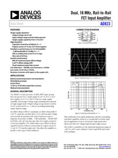
Dual, 16 MHz, Rail-to-Rail FET Input Amplifier Data Sheet ...
www.analog.comCapacitive load drive of 500 pF, G = +1 . Output current of 15 mA, 0.5 V from supplies . Excellent ac performance on 2.6 mA/amplifier . −3 dB bandwidth of 16 MHz, G = +1 . 350 ns settling time to 0.01% (2 V step) Slew rate of 22 V/µs . Good dc performance . 800 µV maximum input offset voltage . 2 µV/°C offset voltage drift . 25 pA maximum ...

350 HO Engine (19210007) Specifications - Chevrolet
www.chevrolet.comTITLE 350 HO Engine (19210007) Specifications REV 28MY14 PART NO. 12366576 DATE REVISION AUTH SHEET OF2 27 30NO99 Initial Release N/A 28AU00Revision N/A 28MY14 Revision - Randall Galagher N/A Legal and Emissions Information This publication is intended to provide information about the 350 HO engine and related components. This

PF2.2: Parents’ use of childbirth-related leave
www.oecd.org350 400 Users/recipients per 100 live births Panel A. Recipients/users of publicly administered parental leave/benefits per 100 live births Men Women 0 10 20 30 40 50 60 70 80 90 100 Share of users/recipients (%) Panel B. Gender distribution of recipients/users of publicly administered parental leave/benefits Men Women

FUSB340 - USB 3.1 SuperSpeed 10 Gbps Switch
www.onsemi.comtON Turn−On Time, S to Output RL = 50 , CL = 0 pF, VSW = 0 V, VSW = 0.6 V 1.5 to 5.0 V − 350 600 ns tOFF Turn−Off Time, S to Output RL = 50 , CL = 0 pF, VSW = 0 V, VSW = 3.3 V 1.5 to 5.0 V − 125 300 ns tZHM,ZL Enable Time, OE to Output RL = 50 , CL = 0 pF, VSW = 0.6 V 1.5 to 5.0 V − 60 150 µs tLZM,HZ Disable Time, OE to Output RL ...
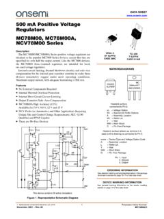
MC78M00 - 500 mA Positive Voltage Regulators
www.onsemi.compF 5.6 k 3.0 k 1.0 k 300 50 200 13 0.24 GND Output 10 pF 2.6 k TO−220 T SUFFIX CASE 221AB 1 DPAK−3 DT SUFFIX CASE 369C MARKINGDIAGRAMS xxxxx = Device Type and Voltage Option Code A = Assembly Location L = Wafer Lot Y = Year WW = Work Week G = Pb−Free Package 2 3 See detailed ordering and shipping information in the package
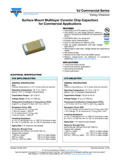
Surface Mount Multilayer Ceramic Chip Capacitors for ...
www.vishay.comVJ Commercial Series www.vishay.com Vishay Vitramon Revision: 10-Apr-2019 1 Document Number: 45199 For technical questions, contact: mlcc@vishay.com THIS DOCUMENT IS SUBJECT TO CHANGE WITHOUT NOTICE.