Design Graphics
Found 5 free book(s)
DRAM Design Overview - Computer Graphics at Stanford ...
www.graphics.stanford.eduDRAM Design Overview Junji Ogawa 90 92 94 96 98 00 02 04 06 08 10 1000 100 20 50 200 500 64M 256M 1G Die Size(mm2) Early Production 256M Production 1G 4G 0.35 0.18 0.13 0.10 Rule (um) Year i-line ArF ? 16M 0.50 64M 0.25 4G KrF 128M KrF+α Standard DRAM Development Conference Feb. 11th. 1998 DRAM Design Overview Junji Ogawa Bit Cost Trend of ...

NVIDIA TESLA P40 GPU ACCELERATOR
www.nvidia.comenabling professional and design engineering workflows at peak performance. The Tesla P40 delivers up to 2X the graphics performance compared to the M60 (Refer to Performance Graph). Users can count on consistent performance with the new resource scheduler, which provides deterministic QoS and eliminates the problem of a “noisy neighbor.”
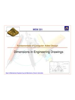
Fundamentals of Computer Aided Design
www.pages.drexel.eduDept of Mechanical Engineering and Mechanics, Drexel University Dimensions • A dimension is for size and position (of the designed/modeled shape). •A DIMENSION is a numerical value expressed in appropriate units of measurement and used to define the size, location, orientation, form
NVIDIA TESLA V100 GPU ARCHITECTURE
images.nvidia.comto power the most computationally intensive HPC, AI, and graphics workloads. The GV100 GPU includes 21.1 billion transistors with a die size of 815 mm2. It is fabricated on a new TSMC 12 nm FFN (FinFET NVIDIA) high-performance manufacturing process customized for NVIDIA.

Datasheet Quadro M2000 - Nvidia
www.nvidia.comadvanced graphics card features an NVIDIA Maxwell™-based GPU, plus 4 GB of ultra-fast on-board memory and the power to drive four 4K displays natively. This makes it an excellent choice for accelerating product development and content creation workflows that demand fluid interactivity with complex models and scenes.