Logic Cross Reference Rev A
Found 6 free book(s)
Hardware and Layout Design Considerations for DDR …
www.nxp.comThe AC logic levels are the points at the receiver where the AC input timing para meters (setup and hold) must be satisfied. The DC logic levels provide a point of hysteresis. When the input level crosses the DC reference point, the receiver switches to the new logic level and maintains this new state as long as the signal does not cross below the

GUIDELINES ON VALIDATION APPENDIX 5 VALIDATION OF ...
www.who.int113 (update - working document QAS/15.639/Rev.1) (2) 114 115 Appendix 2 Validation of water systems for pharmaceutical use116 117 will be replaced by cross-reference to WHO Guidelines on water for pharmaceutical use for consideration in qualification of water purification systems (3)118 119 Appendix 3120 121 Cleaning validation – consensus to ...

Clock Domain Crossing (CDC) Design & Verification ...
www.sunburst-design.comSep 26, 2008 · SNUG Boston 2008 Clock Domain Crossing (CDC) Design & Verification Rev 1.0 Techniques Using SystemVerilog 6 1.0 Introduction In 2001, I presented my first paper on multi-asynchronous clock design.

MPC5744P Data Sheet - NXP
www.nxp.commodel, see the MPC5744P Reference Manual. • Junction temperature: The upper limit is 150°C or 165°C depending on the device marking. NXP Semiconductors Document Number MPC5744P Data Sheet: Technical Data Rev. 6.1, 11/2017 NXP reserves the right to change the production detail specifications as may be
Industry-Standard Dual Operational Amplifiers datasheet ...
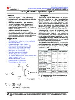
www.ti.com• Programmable logic controllers • Electronic point-of-sale systems RG RF R1 C 1 VIN VOUT = 1 + V V OUT IN R R F G 1 ( ((1 + sRC1 1 1 2p RC1 1 f =-3dB Single-Pole, Low-Pass Filter 3 Description The LM358B and LM2904B devices are the next-generation versions of the industry-standard operational amplifiers (op amps) LM358 and LM2904,

SN65HVD23x 3.3-V CAN Bus Transceivers datasheet (Rev. O)
www.ti.comswitched off in the SN65HVD231 when a high logic level is applied to the RS pin. In this sleep mode the device will not be able to transmit messages to the bus or receive messages from the bus. The device will remain in sleep mode until it is reactivated by applying a …