Operational Amplifier Ac Specifications And Applications
Found 7 free book(s)
OPA657 1.6-GHz, Low-Noise, FET-Input Operational Amplifier ...
www.ti.comOPA657 1.6-GHz, Low-Noise, FET-Input Operational Amplifier 1 Features 3 Description The OPA657 device combines a high-gain bandwidth, ... Specifications transimpedance applications. Photodiode applications ... AC PERFORMANCE (see Figure 29) G = +7 V/V, ...
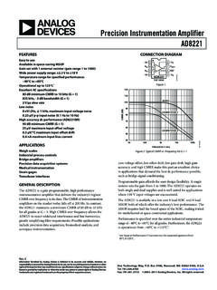
Precision Instrumentation Amplifier AD8221
www.analog.comOperational up to 125°C 1 Excellent AC specifications 80 dB minimum CMRR to 10 kHz (G = 1) 825 kHz, –3 dB bandwidth (G = 1) 2 V/µs slew rate Low noise 8 nV/√Hz, @ 1 kHz, maximum input voltage noise 0.25 µV p-p input noise (0.1 Hz to 10 Hz) High accuracy dc performance (AD8221BR) 90 dB minimum CMRR (G = 1)

High Common-Mode Voltage, Difference Amplifier AD629
www.analog.comThe AD629 is a difference amplifier with a very high input, common-mode voltage range. It is a precision device that allows the user to accurately measure differential signals in the presence of high common-mode voltages up to ±270 V. The AD629 can replace costly isolation amplifiers in applications that do not require galvanic isolation.

AD630 (Rev. G)
www.analog.commentation applications that require wide dynamic range. When used as a synchronous demodulator in a lock-in amplifier configuration, the AD630 can recover a small signal from 100 dB of interfering noise (see the Lock-In Amplifier Applications section). Although optimized for operation up to 1 kHz, the
MCP6001/1R/1U/2/4 - 1 MHz, Low-Power Op Amp
ww1.microchip.comMay 14, 2019 · MCP6001/1R/1U/2/4 DS20001733L-page 4 2002-2020 Microchip Technology Inc. AC ELECTRICAL SPECIFICATIONS TEMPERATURE SPECIFICATIONS Electrical Characteristics: Unless otherwise indicated, TA = +25°C, VDD = +1.8 to 5.5V, VSS = GND, VCM = VDD/2, VL = VDD/2, VOUT VDD/2, RL = 10 k to VL and CL = 60 pF (refer to Figure 1-1). …

2.7V to 5.5V Single Supply CMOS Op Amp
ww1.microchip.comOct 05, 2007 · FIGURE 1-2: AC and DC Test Circuit for Most Non-Inverting Gain Conditions. FIGURE 1-3: AC and DC Test Circuit for Most Inverting Gain Conditions. TEMPERATURE CHARACTERISTICS Electrical Specifications: Unless otherwise indicated, VDD = +2.7V to +5.5V and VSS = GND. Parameters Sym Min Typ Max Units Conditions Temperature Ranges
Op Amps for Everyone Design Guide (Rev. B)
web.mit.eduequations including ac response. The emphasis on single power supply systems forces the designer to bias circuits when the inputs are referenced to ground, and Chapter 4 gives a detailed procedure that quickly yields a working solution every time. Op amps can’t exist without feedback, and feedback has inherent stability problems,