Voltage Converter
Found 8 free book(s)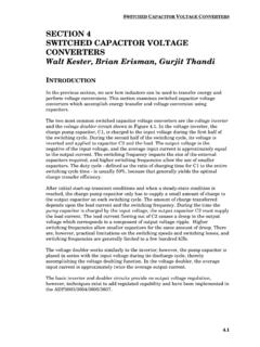
SECTION 4 SWITCHED CAPACITOR VOLTAGE CONVERTERS …
www.analog.comconverters which accomplish energy transfer and voltage conversion using capacitors. The two most common switched capacitor voltage converters are the voltage inverter and the voltage doubler circuit shown in Figure 4.1. In the voltage inverter, the charge pump capacitor, C1, is charged to the input voltage during the first half of the ...
TCS3472 COLOR LIGHT-TO-DIGITAL CONVERTER with IR FILTER
cdn-shop.adafruit.comV INT SDA output low voltage 3 mA sink current 0 0.4 OL INT, SDA output low voltage V 6 mA sink current 0 0.6 ILEAK Leakage current, SDA, SCL, INT pins −5 5 μA ILEAK Leakage current, LDR pin −5 5 μA V SCL SDA input high voltage TCS34721 & TCS34725 0.7 VDD IH SCL, SDA input high voltage V TCS34723 & TCS34727 1.25 V SCL SDA input low voltage
Snubber Circuits Suppress Voltage Transient Spikes in ...
pdfserv.maximintegrated.comConverter Power Supplies Nov 12, 2001 Abstract: The flyback dc-dc converter topology results in significant cost and space savings for multiple output power supplies with high output voltage for power levels up to 100W. Flyback topologies store and transfer energy using a transformer, which due to physical limitations can cause large voltage

Catalog Low voltage Industrial performance motors
library.e.abb.com— Rated voltage U N up to 1000 V — Duty type S1 (continuous duty) or S3 (intermittent periodic duty) with a rated cyclic duration factor of 80 percent or higher — Capable of operating direct online The following motors are excluded from IEC 60034-30: — Motors made solely for converter operation
Basic Calculation of a Buck Converter's Power Stage (Rev. B)
www.ti.comThe output voltage deviation is caused by the time it takes the inductor to catch up with the increased or reduced output current needs. The following formula can be used to calculate the necessary output capacitance for a desired maximum overshoot: 4 Basic Calculation of a Buck Converter's Power Stage SLVA477B–December 2011–Revised August 2015
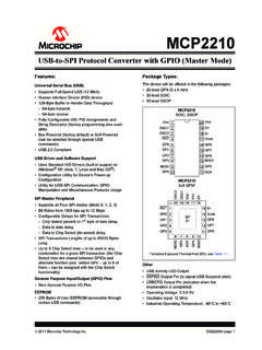
MCP2210 USB-to-SPI Protocol Converter with GPIO (Master …
ww1.microchip.comThe provided V DD voltage has a direct influence on the voltage levels present on the GPIO and SPI module pins (GP8-GP0, MOSI, MISO and SCK). When VDD is 5V, all of these pins will have a logical ‘1’ around 5V with the variations specified in Section 4.1 “DC Char-acteristics”. For applications that require a 3.3V logical ‘1’ level,
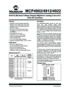
MCP4902/4912/4922 Data Sheet - Microchip Technology
ww1.microchip.com8/10/12-Bit Dual Voltage Output Digital-to-Analog Converter with SPI Interface. MCP4902/4912/4922 DS22250A-page 2 2010 Microchip Technology Inc. Block Diagram Op Amps VDD VSS CS SDI SCK Interface Logic Input Register A Register B DACA Register Register DACB String A DAC B Power-on Reset V OUTA OUTB LDAC Output Gain Logic …

MC34063A, MC33063A, 1.5 A, Step-Up/Down/ Inverting ...
www.sparkfun.comVoltage−Inverting applications with a minimum number of external ... Step−Down Converter 11a. External NPN Switch 11b. External PNP Saturated Switch 8 7 6 Rsc Vin 1 2 Vout 8 7 6 Rsc Vin 1 2 V Figure 11. External Current Boost Connections for IC Peak Greater than 1.5 A. MC34063A, MC33063A, NCV33063A