Transcription of 1/5’’ UXGA CMOS Image Sensor GC2035 DataSheet V1
1 1/5 uxga cmos Image Sensor GC2035 DataSheet 2012-09-18 GalaxyCore Inc. uxga cmos Image Sensor GC2035 DataSheet 2 / 51 Content 1. Sensor OVERVIEW .. 4 GENERAL DESCRIPTION .. 4 FEATURES .. 4 APPLICATION .. 5 TECHNICAL SPECIFICATIONS .. 5 2. BLOCK DIAGRAM .. 6 BLOCK DIAGRAM .. 6 SIGNAL DESCRIPTIONS .. 7 PIN DIAGRAM .. 8 3. OPTICAL SPECIFICATIONS .. 9 Sensor ARRAY CENTER .. 9 PIXEL ARRAY .. 10 LENS CHIEF RAY ANGLE (CRA).. 11 COLOR FILTER SPECTRAL CHARACTERISTICS .. 12 4. TWO-WIRE SERIAL BUS COMMUNICATION.
2 12 PROTOCOL .. 12 SERIAL BUS TIMING .. 13 5. APPLICATIONS .. 14 TIMING DVP .. 14 MIPI .. 15 Clock lane low power .. 15 Data Burst .. 16 uxga cmos Image Sensor GC2035 DataSheet 3 / 51 POWER ON/OFF SEQUENCE .. 17 Power On Sequence .. 17 Power Off Sequence .. 17 DC PARAMETERS .. 17 6. PACKAGE SPECIFICATIONS .. 18 7. REGISTER LIST .. 19 SYSTEM REGISTER .. 19 ANALOG & CISCTL .. 21 ISP RELATED .. 25 uxga cmos Image Sensor GC2035 DataSheet 4 / 51 1.
3 Sensor Overview General Description GC2035 is a high quality 2 Mega cmos Image Sensor , for mobile phone camera applications and digital camera products. GC2035 incorporates a 1616V x 1232H pixel array, on-chip 10-bit ADC, and Image signal processor. The on-chip ISP provides a very smooth AE (Auto Exposure) and accurate AWB (Auto White Balance) control. It provides various data formats, such as Bayer RGB, RGB565, YCbCr 4:2:2. It has a commonly used two-wire serial interface for host to control the operation of the whole Sensor . Internal master clock can be generated by on-chip Phase Lock Loop(PLL) oscillator.
4 Features Standard optical format of 1/5 inch Various output formats: YCbCr4:2:2, RGB565, Raw Bayer PLL support Windowing support MIPI interface support Horizontal /Vertical mirror Image processing module Package: CSP/wafer uxga cmos Image Sensor GC2035 DataSheet 5 / 51 Application Cellular Phone Cameras Notebook and desktop PC cameras PDAs Toys Digital still cameras and camcorders Video telephony and conferencing equipment Security systems Industrial and environmental systems Technical Specifications Parameter Typical value Optical Format 1/5 inch Pixel Size x Active pixel array 1616 x 1232 ADC resolution 10 bit ADC Shutter type Electronic rolling shutter Max Frame rate
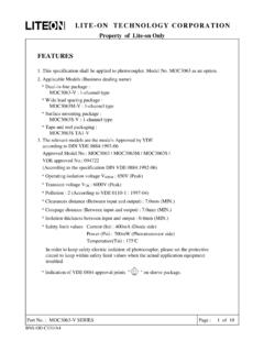
5 15fps@24 Mhz, uxga ~30fps@24 Mhz, SVGA Power Supply AVDD28: ~ DVDD18: ~ IOVDD: ~ Power Consumption 180mW(Active) <100uA(Standby) SNR TBD Dark Current TBD Sensitivity TBD Operating temperature: -20~70 C Stable Image temperature 0~50 C Optimal lens chief ray angle(CRA) 25 non-linear Package type CSP/wafer uxga cmos Image Sensor GC2035 DataSheet 6 / 51 Image Signal Processing Interpolation Denoise Gamma Edge enhanceOutput Mode & Sync Control Pixel Array 1616H x 1232V (1600H x 1200V) Row DecoderColumn CDS Analog Processing 10bit ADC double Timing ControlConfiguration Registers AWBAEC HSYNC VSYNC PCLK YUV/RGB dataRESET SCL MCLK SDA 2.
6 Block Diagram Block Diagram GC2035 has an active Image array of 1616 x 1232 pixels. The active pixels are read out progressively through column/row driver circuits. In order to reduce fixed pattern noise, CDS circuits are adopted. The analog signal is transferred to digital signal by 10 bit A/D converter. The digital signals are processed in the ISP Block, including Bayer interpolation, de-noise, and color correction, gamma correction, and data format conversion and so on. Users can easily control these functions via two-wire serial interface bus. uxga cmos Image Sensor GC2035 DataSheet 7 / 51 Signal Descriptions Name Pin type Description A1 AVDD28 Power Power for analog circuit/ Sensor array A2 PWDN Input power down (active high)
7 A3 SBCL Input SCCB input clock A4 VSYNC Output Vertical reference output A5 PCLK Output Pixel clock output A6 IOVDD Power Power Supply for I/O circuits B1 AGND Ground Ground for analog circuit/ Sensor array B2 RESETB Input reset (active Low) B3 SBDA I/O SCCB data B4 HSYNC Output Horizontal sync output B5 DVDD18 Power Power for digital core B6 D<0> Output YUV/RGB video port bit [0] C1 VPIX Power Internal analog power C2 TXLOW Power internal analog reference C3 NC C4 DGND Ground Ground for digital circuit C5 D<1> Output YUV/RGB video port bit [1] C6 D<2> Output YUV/RGB video port bit [2]
8 D1 CGND Ground Ground for analog circuit D2 AGND Ground Ground for analog circuit/ Sensor array D3 DVDD18 Power Power for digital core D4 DGND Ground Ground for digital circuit D5 D<4> Output YUV/RGB video port bit [4] D6 D<3> Output YUV/RGB video port bit [3] E1 AVDD28 Power Power for analog circuit/ Sensor array uxga cmos Image Sensor GC2035 DataSheet 8 / 51 E2 MDP<0> Output MIPI Data<0> (+) E3 MDN<1> Output MIPI Data<1> (-) E4 MCP Output MIPI clock (+) E5 D<6> Output YUV/RGB video port bit [6] E6 D<5> Output YUV/RGB video port bit [5] F1 INCLK Input Sensor master input clock F2 MDN<0> Output MIPI Data<0> (-) F3 MDP<1> Output MIPI Data<1> (+) F4 MCN Output MIPI clock (-)
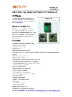
9 F5 D<7> Output YUV/RGB video port bit [7] F6 DVDD18& MVDD Power Power for digital core Power for MIPI Pin Diagram Top View uxga cmos Image Sensor GC2035 DataSheet 9 / 51 3. Optical Specifications Sensor Array Center Top View uxga cmos Image Sensor GC2035 DataSheet 10 / 51 Pixel Array Pixel array is covered by Bayer pattern color filters.
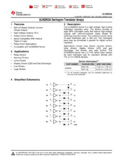
10 The primary color BG/GR array is arranged in line-alternating way. If no flip in column, column is read out from 0 to 1615. If flip in column, column is read out from 1615 to 0. If no flip in row, row is read out from 0 to 1231. If flip in row, row is read out from 1231to 0. uxga cmos Image Sensor GC2035 DataSheet 11 / 51 Lens Chief Ray Angle (CRA) Image Height (mm) Field (%) Image height(mm) CRA(degrees) 0 0 0 10 20 30 40 50 60 70 80 90 100 110 uxga cmos Image Sensor GC2035 DataSheet 12 / 51 Color Filter Spectral Characteristics The optical spectrum of color filters is shown as follows: 4.