Transcription of 120V-100W DMOS AUDIO AMPLIFIER WITH …
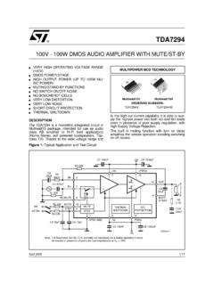
1 TDA7293120V - 100w DMOS AUDIO AMPLIFIER with mute /ST-BYVERY HIGH OPERATING VOLTAGE RANGE( 50V)DMOS POWER STAGEHIGH OUTPUT POWER ( 100w @ THD =10%, RL=8 ,VS= 40V)MUTING/STAND-BY FUNCTIONSNO SWITCH ON/OFF NOISEVERY LOW DISTORTIONVERY LOW NOISESHORT CIRCUIT PROTECTIONTHERMAL SHUTDOWNCLIP DETECTORMODULARITY (MORE DEVICES CAN BEEASILY CONNECTED IN PARALLEL TODRIVE VERY LOW IMPEDANCES)DESCRIPTIONThe TDA7293 is a monolithic integrated circuit inMultiwatt15 package, intended for use as audioclass AB AMPLIFIER in Hi-Fi field applications(Home Stereo, self powered loudspeakers, Top-class TV). Thanks to the wide voltage range andto the high out current capability it is able to sup-ply the highest power into both 4 and 8 built in muting function with turn on delaysimplifies the remote operation avoiding switchingon-off mode is made possible by connectingmore device through of pin11.
2 High output powercan be delivered to very low impedance loads, sooptimizing the thermal dissipation of the IN-2R2 680 C2 22 FC1 470nFIN+R1 22K3R3 22K-+MUTESTBY4 VMUTEVSTBY109 SGNDMUTESTBYR4 22 KTHERMAL SHUTDOWNS/C PROTECTIONR5 10KC3 10 FC410 F1 STBY-GNDC5 22 F713146158-Vs-PWVsBOOTSTRAPOUT+PWVs+VsC9 100nFC8 1000 F-VsD97AU805A+VsC7 100nFC6 1000 FBUFFER DRIVER11 BOOT LOADER125 VCLIPCLIP DET(*)(*) see Applicationnote (**) for SLAVE function(**)Figure 1:Typical Application and Test CircuitMultiwatt15 ORDERING NUMBER:TDA7293 VMULTIPOWER BCD TECHNOLOGY1/13 ABSOLUTE MAXIMUM RATINGSS ymbolParameterValueUnitVSSupply Voltage (No Signal) 60VV1 VSTAND-BYGND Voltage Referred to -VS(pin 8)90VV2 Input Voltage (inverting) Referred to -VS90VV2-V3 Maximum Differential Inputs 30VV3 Input Voltage (non inverting)
3 Referred to -VS90VV4 Signal GND Voltage Referred to -VS90VV5 Clip Detector Voltage Referred to -VS120VV6 Bootstrap Voltage Referred to -VS120VV9 Stand-by Voltage Referred to -VS120VV10 mute Voltage Referred to -VS120VV11 Buffer Voltage Referred to -VS120VV12 Bootstrap Loader Voltage Referred to -VS100 VIOO utput Peak Current10 APtotPower Dissipation Tcase=70 C50 WTopOperating Ambient Temperature Range0 to 70 CTstg,TjStorage and Junction Temperature150 C1234567910118 BUFFER DRIVERMUTESTAND-BY-VS(SIGNAL)+VS(SIGNAL) BOOTSTRAPCLIP AND SHORT CIRCUIT DETECTORSIGNAL GROUNDNON INVERTING INPUTINVERTING INPUTSTAND-BY GNDTAB CONNECTED TO PIN 813141512-VS(POWER)OUT+VS(POWER)BOOTSTRA P LOADERD97AU806 PIN CONNECTION(Top view)QUICK REFERENCE DATAS ymbolParameterTest Voltage Operating 12 50 VGLOOPC losed Loop Gain2640dBPtotOutput PowerVS= 45V; RL=8 ; THD = 10%140 WVS= 30V; RL=4 ; THD = 10%110 WSVRS upply Voltage Rejection75dBTHERMAL DATAS ymbolDescriptionTypMaxUnitRth j-caseThermal Resistance C/WTDA72932/13 ELECTRICAL CHARACTERISTICS(Refer to the Test Circuit VS= 40V, RL=8 ,Rg=50 ;Tamb=25 C, f = 1 kHz; unless otherwise specified).
4 SymbolParameterTest Range 12 50 VIqQuiescent Current30mAIbInput Bias AVOSI nput Offset Voltage-1010mVIOSI nput Offset APORMS Continuous Output Powerd = 1%:RL=4 ; VS= 29V,8080Wd = 10%RL=4 ;VS= 29V100100 WdTotal Harmonic Distortion (**)PO= 5W; f = 1kHzPO= to 50W; f = 20Hz to Limiter Rate15V/ sGVOpen Loop Voltage Gain80dBGVC losed Loop Voltage Gain (1)30dBeNTotal Input NoiseA = curvef = 20Hz to 20kHz125 V VRiInput Resistance100k SVRS upply Voltage Rejectionf = 100Hz; Vripple= ProtectionDEVICE MUTED150 CDEVICE SHUT DOWN160 CSTAND-BY FUNCTION(Ref: to pin 1)VST onStand-by on of fStand-by off Attenuation7090dBIq st-byQuiescent Current @ FUNCTION(Ref: to pin 1)VMonMute on off AttenuatIon6080dBCLIP DETECTORDutyDuty Cycle ( pin 5)THD = 1% ; RL = 10K to 5V10%THD = 10% ;RL = 10K to 5V40%ICLEAKPO = 50W1 ASLAVE FUNCTION pin 4(Ref: to pin 8 -VS)VSlaveSlaveThreshold1 VVMasterMaster Threshold3 VNote (1):GVmin 26dBNote:Pin 11 only for modular connection.
5 Max external load 1M /10 pF, only for test purposeNote (**):Tested with optimized Application Board (see fig. 2)TDA72933/13 Figure 2:Typical Application Board and Component Layout (scale 1:1)TDA72934/13 APPLICATION SUGGESTIONS(see Test and Application Circuits of the Fig. 1)The recommended values of the external components are those shown on the application circuit of Fig-ure 1. Different values can be used; the following table can help the VALUEPURPOSELARGER THANSUGGESTEDSMALLER THANSUGGESTEDR1 (*)22kINPUT RESISTANCEINCREASE INPUTIMPEDANCEDECREASE INPUTIMPEDANCER2680 CLOSED LOOP GAINSET TO 30dB (**)DECREASE OF GAIN INCREASE OF GAINR3 (*)22kINCREASE OF GAIN DECREASE OF GAINR422kST-BY TIMECONSTANTLARGER ST-BYON/OFF TIMESMALLER ST-BYON/OFF TIME;POP NOISER510kMUTE TIMECONSTANTLARGER MUTEON/OFF TIMESMALLER MUTEON/OFF FINPUT DCDECOUPLINGHIGHER LOWFREQUENCYCUTOFFC222 FFEEDBACK DCDECOUPLINGHIGHER LOWFREQUENCYCUTOFFC310 FMUTE TIMECONSTANTLARGER MUTEON/OFF TIMESMALLER MUTEON/OFF TIMEC410 FST-BY TIMECONSTANTLARGER ST-BYON/OFF TIMESMALLER ST-BYON/OFF TIME.
6 POP NOISEC522 FXN (**)BOOTSTRAPPINGSIGNALDEGRADATION ATLOW FREQUENCYC6, C81000 FSUPPLY VOLTAGEBYPASSC7, FSUPPLY VOLTAGEBYPASSDANGER OFOSCILLATION(*) R1 = R3 for pop optimization(**) Closed Loop Gain has to be 26dB(**) Multiplay this value for the number of modular part connectedMASTERUNDEFINEDSLAVE-VS+3V-VS+1 V-VSD98AU821 Slave function: pin 4 (Ref to pin 8 -VS)Note:If in the application, the speakers are connectedvia long wires, it is a good rule to add betweenthe output and GND, a Boucherot Cell, in order toavoid dangerous spurious oscillations when thespeakers terminal are suggested Boucherot Resistor is /2 Wand the capacitor is 1 consumer electronics, an increasing demandhas arisen for very high power monolithic audioamplifiers able to match, with a low cost, the per-formance obtained from the best discrete task of realizing this linear integrated circuitin conventional bipolar technology is made ex-tremely difficult by the occurence of 2nd break-down phoenomenon.
7 It limits the safe operatingarea (SOA) of the power devices, and, as a con-sequence, the maximum attainable output power,especially in presence of highly reactive , full exploitation of the SOA translatesinto a substantial increase in circuit and layoutcomplexity due to the need of sophisticated pro-tection overcome these substantial drawbacks, theuse of power MOS devices, which are immunefrom secondary breakdown is highly device described has therefore been devel-oped in a mixed bipolar-MOS high voltage tech-nology called BCDII 100 ) Output StageThe main design task in developping a power op-erational AMPLIFIER , independently of the technol-ogy used, is that of realization of the output solution shown as a principle shematic byFig3 represents the DMOS unity - gain outputbuffer of the large-signal, high-power buffer must be ca-pable of handling extremely high current and volt-age levels while maintaining acceptably low har-monic distortion and good behaviour overfrequency response.
8 Moreover, an accurate con-trol of quiescent current is local linearizing feedback, provided by differen-tial AMPLIFIER A, is used to fullfil the above require-ments, allowing a simple and effective quiescentcurrent biasing of the power output transistorsalone is however not enough to guarantee the ab-sence of crossover a linearization of the DC transfer charac-teristic of the stage is obtained, the dynamic be-haviour of the system must be taken into significant aid in keeping the distortion contrib-uted by the final stage as low as possible is pro-vided by the compensation scheme, which ex-ploits the direct connection of the Miller capacitorat the AMPLIFIER s output to introduce a local ACfeedback path enclosing the output stage )
9 ProtectionsIn designing a power IC, particular attention mustbe reserved to the circuits devoted to protectionof the device from short circuit or overload to the absence of the 2nd breakdown phe-nomenon, the SOA of the power DMOS transis-tors is delimited only by a maximum dissipationcurve dependent on the duration of the order to fully exploit the capabilities of thepower transistors, the protection scheme imple-mented in this device combines a conventionalSOA protection circuit with a novel local tempera-ture sensing technique which dynamically con-trols the maximum 3:Principle Schematic of a DMOS unity-gain addition to the overload protection describedabove, the device features a thermal shutdowncircuit which initially puts the device into a mutingstate (@ Tj = 150oC) and then into stand-by (@Tj = 160oC).
10 Full protection against electrostatic discharges onevery pin is ) Other FeaturesThe device is provided with both stand-by andmute functions, independently driven by twoCMOS logic compatible input circuits dedicated to the switching on and offof the AMPLIFIER have been carefully optimized toavoid any kind of uncontrolled audible transient atthe sequence that we recommend during theON/OFF transients is shown by Figure application of figure 5 shows the possibility ofusing only one command for both st-by and mutefunctions. On both the pins, the maximum appli-cable range corresponds to the operating INFORMATIONHIGH-EFFICIENCYC onstraints of implementing high power solutionsare the power dissipation and the size of thepower supply.