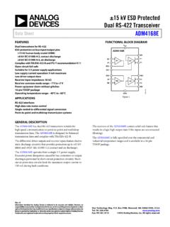
Transcription of 15 kV ESD protected, 3 to 5.5 V low power, up to 250 Kbps ...
1 January 2008 Rev 81/1515ST3222 EBST3222EC 15 kv ESD protected , 3 to Vlow power, up to 250 Kbps, RS-232 drivers and receiversFeatures ESD protection for RS-232 I/O pins 15 kv human body model, 8 kV IEC 1000-4-2 contact discharge 300 A supply current 250 KBps minimum guarantee data rate 6 V/ s minimum guarantee slew rate Meet EIA/TIA-232 specification down to 3 V Available in SSOP20 and TSSOP20 DescriptionThe ST3222E is a 3 V powered EIA/TIA-232 and communications interface with low power requirements, high data-rate capabilities and enhanced electrostatic discharge (ESD) protection to 8 kV using IEC1000-4-2 Contact Discharge and 15 kv using the Human Body Model. ST3222E has a proprietary low dropout transmitter output stage providing true RS-232 performance from 3 to 5 V supplies with a dual charge pump. The charge pump requires only four small mF external capacitors for operation form 3 V supply.
2 The device has two receivers and two drivers. The ST3222E features a 1 mA shutdown mode that reduces power consumption and extends battery life in portable systems. Its receivers can remain active in shutdown mode, allowing external devices such as modems to be monitored using only 1 mA supply current. The device is guaranteed to run at data rates of 250 Kbps while maintaining RS-232 output applications are Notebook, Sub-notebook and Palmtop Computers, Battery Powered Equipment, Hand-Held Equipment, Peripherals and summaryOrder codesTemperature rangePackagePackagingST3222 ECPR0 to 70 CSSOP20 (tape and reel)1350 parts per reelST3222 EBPR-40 to 85 CSSOP20 (tape and reel)1350 parts per reelST3222 ECTR0 to 70 CTSSOP20 (tape and reel)2500 parts per reelST3222 EBTR-40 to 85 CTSSOP20 (tape and reel)2500 parts per Contents1 Pin configuration .. 32 Absolute maximum ratings.
3 43 Electrical characteristics .. 54 Application circuits .. 75 Typical performance characteristics .. 86 Package mechanical data .. 97 Revision history .. 14ST3222 EPin configuration3/151 Pin configuration Figure connection Table descriptionPin n SymbolName and function1 ENReceiver enable control. drive low for normal operation. Drive high to force the receivers outputs (R_OUT) into a high-impedance +Positive terminal for the first charge pump capacitor3V+ Generated by the charge terminal for the first charge pump capacitor5C2+Positive terminal for the second charge pump capacitor6C2-Negative terminal for the second charge pump Generated by the charge transmitter output voltage9R2 INSecond receiver input voltage10R2 OUTS econd receiver output voltage11 NCNot connected12T2 INSecond transmitter input voltage13T1 INFirst transmitter input voltage14 NCNot connected15R1 OUTF irst receiver output voltage16R1 INFirst receiver input voltage17T1 OUTF irst transmitter output voltage18 GNDG round19 VCCS upply voltage20 SHDNA ctive low shutdown control input.
4 Drive low to shut-down transmitter and charge pumpAbsolute maximum ratingsST3222E4/15 2 Absolute maximum ratings Note:Absolute maximum ratings are those values beyond which damage to the device may occur. Functional operation under these condition is not applied V+ and V- can have a maximum magnitude of +7 V, but their absolute addition can not exceed 13 on internal charge pump, intrinsic self limitation allows exceeding those values without any voltage sequence (VCC, then V+, then V-) is critical, therefore it is not recommended to use this device using externally applied voltage to V+ and V-. Table maximum ratingsSymbolParameterValueUnitVCCS upply to 6VV+Doubled voltage terminal(VCC - ) to 7VV-Inverted voltage to -7VV+ +|V-|13 VTINT ransmitter input voltage to 6 VRINR eceiver input voltage range 25 VTOUTT ransmitter output voltage range output voltage to (VCC + )VtSHORTT ransmitter output short to gnd timeContinuousTable and enable control truth tableSHDNENT-OUTR-OUT00 High ZActive01 High ZHigh Z10 ActiveActive11 ActiveHigh ZTable performance: transmitter outputs, receiver inputsSymbolParameterTest protection voltageHuman body model 15kVESDESD protection voltageIEC-1000-4-2 8kVST3222 EElectrical characteristics5/153 Electrical characteristics Note:1 Transmitter input hysteresis is typically 250 mV Table characteristics (C1 - C4 = F, VCC = 3 V to V, TA = -40 to 85 C, unless otherwise specified.)
5 Typical values are referred to TA = 25 C)SymbolParameterTest power supply current No load, SHDN = VCC, TA = 25 supply currentNo load, SHDN = VCC, TA = 25 C110 ATable input electrical characteristics (C1 - C4 = F, VCC = 3 V to V,TA = -40 to 85 C, unless otherwise specified. Typical values are referred to TA = 25 C)SymbolParameterTest logic threshold lowT-IN, EN, SHDN (Note: 1) logic threshold highVCC = V2 VVCC = 5 input leakage currentT-IN, EN, SHDN 1 ATable electrical characteristics (C1 - C4 = F VCC = 3 V to V, TA = -40 to 85 C, unless otherwise specified. Typical values are referred to TA = 25 C)SymbolParameterTest voltage swingAll transmitter outputs are loaded with 3 K to GND 5 output resistanceVCC = V+ = V- = 0 V, VOUT = 2 V30010M ITSCO utput short circuit current 60mAITOLO utput leakage currentVCC = 0 or 3 V to V, VOUT = 12 V Transmitters disable 25 AElectrical characteristicsST3222E6/15 Table electrical characteristics (C1 - C4 = F, VCC = 3 V to V, TA = -40 to 85 C, unless otherwise specified.
6 Typical values are referred to TA = 25 C)SymbolParameterTest leakage currentR-OUT, EN = VCC, receiver disabled 10 AVRINR eceiver input voltage operating range-2525 VVRILI nput threshold lowTA = 25 C, VCC = = 25 C, VCC = 5 threshold highTA = 25 C, VCC = = 25 C, VCC = 5 resistanceTA = 25 C357K VROLO utput voltage lowIOUT = voltage highIOUT = -1 characteristics (C1 - C4 = F, VCC = 3 V to V, TA = -40 to 85 C, unless otherwise specified. Typical values are referred to TA = 25 C)SymbolParameterTest transfer rateRL = 3 K , CL2= 1000 pFone transmitter switching250 KbpstPHLR tPLHRP ropagation delay input to output RXIN to RXOUT, CL = 150 s|tPHLT- tTHL|Transmitter propagation delay difference (1)200nstOERR eceiver output enable timeNormal operation50nstODRR eceiver output disable timeNormal operation50ns|tPHLR- tTHR|Receiver propagation delay difference 50nsSRTT ransition slew rateTA = 25 C RL = 3 K to 7 K VCC = Vmeasured from +3V to -3V or -3V to +3 VCL = 150 pF to 1000 pF630V/ sTA = 25 C RL = 3 K to 7 K VCC = Vmeasured from +3V to -3V or -3V to +3 VCL = 150 pF to 2500 pF430V/ s1.
7 Transmitter Skew is measured at the transmitter zero cross pointsST3222 EApplication circuits7/154 Application circuits Figure schematic Table value ( F) to to to performance characteristicsST3222E8/15 5 Typical performance characteristics(unless otherwise specified TJ = 25 C) Figure current vs output high voltageFigure current vs output high voltage Figure current vs output low voltageFigure current vs output low voltage Figure transfer characteristics for transmitter inputsFigure input resistance ST3222 EPackage mechanical data9/156 Package mechanical dataIn order to meet environmental requirements, ST offers these devices in ECOPACK packages. These packages have a lead-free second level interconnect. The category of second level interconnect is marked on the package and on the inner box label, in compliance with JEDEC Standard JESD97.
8 The maximum ratings related to soldering conditions are also marked on the inner box label. ECOPACK is an ST trademark. ECOPACK specifications are available at: mechanical dataST3222E10/15 BSCK0 4 8 0 4 8 mechanical datacEbA2AE1D1 PIN 1 IDENTIFICATIONA1 LKe0061436 CST3222 EPackage mechanical data11/15 BSCK0 8 0 8 mechanical datacEbA2AE1D1 PIN 1 IDENTIFICATIONA1 LKe0087225 CPackage mechanical dataST3222E12/15 & reel SSOP20 mechanical dataST3222 EPackage mechanical data13/15 & reel TSSOP20 mechanical dataRevision historyST3222E14/15 7 Revision history Table revision historyDateRevisionChanges22-Mar-20066 Order codes Ta b l e 1 in cover note on Ta b l e Please Read Carefully:Information in this document is provided solely in connection with ST products. STMicroelectronics NV and its subsidiaries ( ST ) reserve theright to make changes, corrections, modifications or improvements, to this document, and the products and services described herein at anytime, without ST products are sold pursuant to ST s terms and conditions of are solely responsible for the choice, selection and use of the ST products and services described herein, and ST assumes noliability whatsoever relating to the choice, selection or use of the ST products and services described license, express or implied, by estoppel or otherwise, to any intellectual property rights is granted under this document.
9 If any part of thisdocument refers to any third party products or services it shall not be deemed a license grant by ST for the use of such third party productsor services, or any intellectual property contained therein or considered as a warranty covering the use in any manner whatsoever of suchthird party products or services or any intellectual property contained OTHERWISE SET FORTH IN ST S TERMS AND CONDITIONS OF SALE ST DISCLAIMS ANY EXPRESS OR IMPLIEDWARRANTY WITH RESPECT TO THE USE AND/OR SALE OF ST PRODUCTS INCLUDING WITHOUT LIMITATION IMPLIEDWARRANTIES OF MERCHANTABILITY, FITNESS FOR A PARTICULAR PURPOSE (AND THEIR EQUIVALENTS UNDER THE LAWSOF ANY JURISDICTION), OR INFRINGEMENT OF ANY PATENT, COPYRIGHT OR OTHER INTELLECTUAL PROPERTY EXPRESSLY APPROVED IN WRITING BY AN AUTHORIZED ST REPRESENTATIVE, ST PRODUCTS ARE NOTRECOMMENDED, AUTHORIZED OR WARRANTED FOR USE IN MILITARY, AIR CRAFT, SPACE, LIFE SAVING, OR LIFE SUSTAININGAPPLICATIONS, NOR IN PRODUCTS OR SYSTEMS WHERE FAILURE OR MALFUNCTION MAY RESULT IN PERSONAL INJURY,DEATH, OR SEVERE PROPERTY OR ENVIRONMENTAL DAMAGE.
10 ST PRODUCTS WHICH ARE NOT SPECIFIED AS "AUTOMOTIVEGRADE" MAY ONLY BE USED IN AUTOMOTIVE APPLICATIONS AT USER S OWN of ST products with provisions different from the statements and/or technical features set forth in this document shall immediately voidany warranty granted by ST for the ST product or service described herein and shall not create or extend in any manner whatsoever, anyliability of and the ST logo are trademarks or registered trademarks of ST in various in this document supersedes and replaces all information previously ST logo is a registered trademark of STMicroelectronics. All other names are the property of their respective owners. 2008 STMicroelectronics - All rights reservedSTMicroelectronics group of companiesAustralia - Belgium - Brazil - Canada - China - Czech Republic - Finland - France - Germany - Hong Kong - India - Israel - Italy - Japan - Malaysia - Malta - Morocco - Singapore - Spain - Sweden - Switzerland - United Kingdom - United States of
