Transcription of 15 MHz Rail-to-Rail Operational Amplifiers Data Sheet ...
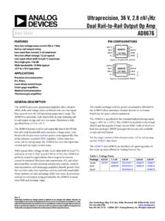
1 15 MHz Rail-to-Rail Operational Amplifiers Data Sheet op162 /OP262/OP462. FEATURES PIN CONFIGURATIONS. Wide bandwidth: 15 MHz NULL 1 8 NULL. Low offset voltage: 325 V max IN A 2 op162 7 V+. Low noise: nV/ Hz @ 1 kHz +IN A 3 TOP VIEW 6 OUT A. Single-supply operation: V to 12 V V 4 (Not to Scale) 5 NC. 00288-001. Rail-to-Rail output swing NC = NO CONNECT. Low TCVOS: 1 V/ C typ High slew rate: 13 V/ s Figure 1. 8-Lead Narrow-Body SOIC (S Suffix). No phase inversion OUT A V+. Unity-gain stable 1 8. IN A 2 OP262 7 OUT B.
2 APPLICATIONS +IN A 3. TOP VIEW. (Not to Scale). 6 IN B. 00288-004. Portable instrumentation V 4 5 +IN B. Sampling ADC amplifier Wireless LANs Figure 2. 8-Lead TSSOP (RU Suffix) and 8-Lead Narrow-Body SOIC (S Suffix). Direct access arrangement Office automation OUT A 1 14 OUT D. IN A 2 13 IN D. +IN A 3 OP462 12 +IN D. GENERAL DESCRIPTION V+ 4. TOP VIEW. (Not to Scale). 11 V . The op162 (single), OP262 (dual), and OP462 (quad) rail -to- +IN B 5 10 +IN C. rail 15 MHz Amplifiers feature the extra speed new designs IN B 6 9 IN C.
3 00288-006. require, with the benefits of precision and low power operation. OUT B 7 8 OUT C. With their incredibly low offset voltage of 45 V (typical) and Figure 3. 14-Lead Narrow-Body SOIC (S Suffix) and low noise, they are perfectly suited for precision filter applica- 14-Lead TSSOP (RU Suffix). tions and instrumentation. The low supply current of 500 A. (typical) is critical for portable or densely packed designs. In addition, the Rail-to-Rail output swing provides greater dynamic range and control than standard video Amplifiers .
4 These products operate from single supplies as low as V to dual supplies of 6 V. The fast settling times and wide output swings recommend them for buffers to sampling A/D converters. The output drive of 30 mA (sink and source) is needed for many audio and display applications; more output current can be supplied for limited durations. The OPx62 family is specified over the extended industrial temperature range ( 40 C to +125 C). The single op162 Amplifiers are available in 8-lead SOIC package. The dual OP262 Amplifiers are available in 8-lead SOIC and TSSOP packages.
5 The quad OP462 Amplifiers are available in 14-lead, narrow-body SOIC and TSSOP. packages. Rev. H Document Feedback Information furnished by analog devices is believed to be accurate and reliable. However, no responsibility is assumed by analog devices for its use, nor for any infringements of patents or other rights of third parties that may result from its use. Specifications subject to change without notice. No One Technology Way, Box 9106, Norwood, MA 02062-9106, license is granted by implication or otherwise under any patent or patent rights of analog devices .
6 Tel: 2013 analog devices , Inc. All rights reserved. Trademarks and registered trademarks are the property of their respective owners. Technical Support op162 /OP262/OP462 Data Sheet TABLE OF CONTENTS. Features .. 1 Input Overvoltage Protection .. 13. Applications .. 1 Output Phase Reversal .. 13. General Description .. 1 Power 13. Pin Configurations .. 1 Unused Amplifiers .. 14. Revision History .. 2 Power-On Settling Time .. 14. 3 Capacitive Load Drive .. 14. Absolute Maximum Ratings .. 6 Total Harmonic Distortion and Crosstalk.
7 15. ESD Caution .. 6 PCB Layout Considerations .. 15. Typical Performance Characteristics .. 7 Applications 16. Applications .. 12 Single-Supply Stereo Headphone 16. Functional Description .. 12 Instrumentation 16. Offset Adjustment .. 12 Direct Access Arrangement .. 17. Rail-to-Rail Output .. 12 Outline Dimensions .. 18. Output Short-Circuit Protection .. 12 Ordering Guide .. 20. REVISION HISTORY. 4/13 Rev. G to Rev. H 12/04 Rev. D to Rev. E. Combined Figure 2 and Figure 3; Combined Figure 4 and Updated Format.
8 Universal Figure 5 .. 1 Changes to General Description ..1. Changes to Figure 12 .. 9 Changes to Specifications ..3. 5/12 Rev. F to Rev. G Changes to Package Type ..6. Change to Figure 16 ..8. Deleted MSOP Throughout .. 1 Change to Figure 22 ..9. Deleted Figure 2; Renumbered 1 Change to Figure 36 .. 13. Deleted Spice-Macro Model Section .. 18 Change to Figure 37 .. 14. Updated Outline Dimensions .. 18 Changes to Ordering Guide .. 20. Changes to Ordering Guide .. 20. 10/02 Rev. C to Rev. D. 1/05 Rev.
9 E to Rev. F. Deleted 8-Lead Plastic DIP (N-8) .. Universal Changes to Absolute Maximum Ratings Table 4 and Table 5 .. 6 Deleted 14-Lead Plastic DIP (N-14) .. Universal Change to Figure 36 .. 13 Edits to ORDERING GUIDE .. 19. Changes to Ordering Guide .. 20 Edits to Figure 30 .. 19. Edits to Figure 31 .. 19. Updated Outline Dimensions .. 19. Rev. H | Page 2 of 20. Data Sheet op162 /OP262/OP462. SPECIFICATIONS. @ VS = V, VCM = 0 V, TA = 25 C, unless otherwise noted. Table 1. Electrical Characteristics Parameter Symbol Conditions Min Typ Max Unit INPUT CHARACTERISTICS.
10 Offset Voltage VOS OP162G, OP262G, OP462G 45 325 V. 40 C TA +125 C 800 V. H grade, 40 C TA +125 C 1 mV. D grade 3 mV. 40 C TA +125 C 5 mV. Input Bias Current IB 360 600 nA. 40 C TA +125 C 650 nA. Input Offset Current IOS 25 nA. 40 C TA +125 C 40 nA. Input Voltage Range VCM 0 4 V. Common-Mode Rejection CMRR 0 V VCM V, 40 C TA +125 C 70 110 dB. Large Signal Voltage Gain AVO RL = 2 k , VOUT V 30 V/mV. RL = 10 k , VOUT V 65 88 V/mV. RL = 10 k , 40 C TA +125 C 40 V/mV. Long-Term Offset Voltage 1 VOS G grade 600 V.