Transcription of ±15 kV ESD Protected, 3.3 V Single- Channel RS-232 …
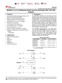
1 15 kV ESD Protected, V Single- Channel RS-232 line Driver/ receiver data sheet adm3101e . FEATURES FUNCTIONAL BLOCK DIAGRAM. + INPUT. 460 kbps data rate 1 Tx and 1 Rx C1 + C1+ VCC. + TO + + C5. Meets EIA/TIA-232E specifications F VOLTAGE DOUBLER + C3. 16V F F. C1 V+ F charge pump capacitors C2+ V . Contact discharge: 8 kV C2 +. + TO F + C4. VOLTAGE INVERTER F. Air gap discharge: 15 kV 16V C2 16V. TIN TOUT. CMOS EIA/TIA-232E. APPLICATIONS INPUT T OUTPUT. General-purpose RS-232 data links adm3101e . ROUT RIN. Industrial/telecommunications diagnostics ports CMOS R EIA/TIA-232E. OUTPUT INPUT*. GND. 06766-001. *INTERNAL 5k PULL-DOWN. RESISTOR ON THE RS-232 INPUT. Figure 1. GENERAL DESCRIPTION. The adm3101e is a high speed, single- Channel , RS-232 / Because of the 15 kV ESD protection of the adm3101e . ITU-T transceiver interface device that operates from input/output pins, this device is ideally suited for operation a single V power supply. Low power consumption makes in electrically harsh environments or where RS-232 cables are it ideal for battery-powered portable instruments.
2 Frequently plugged and unplugged. The adm3101e conforms to the EIA/TIA-232E and ITU-T Four external F charge pump capacitors are used for the specifications and operates at data rates of up to 460 kbps. voltage doubler/inverter permitting operation from a single All RS-232 (TOUT and RIN) and CMOS (TIN and ROUT) inputs V supply. and outputs are protected against electrostatic discharges (up The adm3101e is available in both a 12-lead LFCSP and 16-lead to 15 kV ESD protection). QSOP, specified over the 40 C to +85 C temperature range. Rev. D Document Feedback Information furnished by analog devices is believed to be accurate and reliable. However, no responsibility is assumed by analog devices for its use, nor for any infringements of patents or other rights of third parties that may result from its use. Specifications subject to change without notice. No One Technology Way, Box 9106, Norwood, MA 02062-9106, license is granted by implication or otherwise under any patent or patent rights of analog devices .
3 Tel: 2007 2015 analog devices , Inc. All rights reserved. Trademarks and registered trademarks are the property of their respective owners. Technical Support adm3101e data sheet TABLE OF CONTENTS. Features .. 1 Pin Configurations and Function Descriptions ..5. Applications .. 1 Typical Performance Characteristics ..6. Functional Block Diagram .. 1 Theory of Operation ..8. General Description .. 1 Circuit Description ..8. Revision History .. 2 High Baud Rate ..8. 3 Outline Dimensions ..9. Absolute Maximum 4 Ordering Guide ..9. ESD Caution .. 4. REVISION HISTORY. 5/15 Rev. C to Rev. D 10/07 Rev. 0 to Rev. A. Change to JA, Thermal Impedance (LFCSP) Parameter, Changes to Figure 1 ..1. Table 2 .. 4 Changes to Table 1, RS-232 receiver Section ..3. Changes to Figure 2 and Table 3 .. 5 Changes to Table Changes to Ordering Guide .. 9 Changes to Figure Updated Outline Dimensions .. 9. 5/07 Revision 0: Initial Version 7/08 Rev. B to Rev. C. Changes to General Description Section.
4 1. Reformatted Table 1 .. 4. Change to TIN Rating, Table 2 .. 4. Changes to Figure 2 .. 5. Moved High Baud Rate Section .. 8. Added Exposed Pad Notation to Outline Dimensions .. 9. 12/07 Rev. A to Rev. B. Added 16-Lead QSOP Package (Universal) .. 1. Updated Outline Dimensions .. 10. Changes to Ordering Guide .. 10. Rev. D | Page 2 of 12. data sheet adm3101e . SPECIFICATIONS. VCC = V V, C1 to C4 = F, 40 C TA +85 C, unless otherwise noted. Table 1. Parameter Test Conditions/Comments Min Typ Max Unit DC CHARACTERISTICS. Operating Voltage Range V. Power Supply Current, VCC No load mA. RL = 3 k to GND 5 7 mA. LOGIC. Input Logic Threshold Low, VINL TIN V. Input Logic Threshold High, VINH TIN V. Input Logic Threshold Low, VINL TIN, VCC = V V V. Input Logic Threshold High, VINH TIN, VCC = V V V. CMOS Output Voltage Low, VOL IOUT = mA V. CMOS Output Voltage High, VOH IOUT = 1 mA VCC V. Logic Pull-Up Current TIN = GND to VCC 5 12 A. RS-232 receiver .
5 EIA/TIA-232E Input Voltage Range1 30 +30 V. EIA/TIA-232E Input Threshold Low VCC = V to V V. EIA/TIA-232E Input Threshold High V. EIA/TIA-232E Input Hysteresis V. EIA/TIA-232E Input Resistance 3 5 7 k . TRANSMITTER. Output Voltage Swing RS-232 VCC = V to V; transmitter output loaded V. with 3 k to ground RS-562 VCC = V V. Transmitter Output Resistance VCC = 0 V, VOUT = 2 V1 300 . RS-232 Output Short-Circuit Current 15 mA. TIMING CHARACTERISTICS. Maximum data Rate VCC = V, RL = 3 k to 7 k , CL = 50 pF to 1000 pF 460 kbps receiver Propagation Delay tPHL s tPLH s Transmitter Propagation Delay RL = 3 k , CL = 1000 pF 600 ns Transmitter Skew 80 ns receiver Skew 70 ns Transition Region Slew Rate +3 V to 3 V or 3 V to +3 V, VCC = + V, 10 30 V/ s RL = 3 k , CL = 1000 pF, TA = 25 C1. ESD PROTECTION. RS-232 and CMOS I/O Pins Human body model air discharge 15 kV. Human body model contact discharge 8 kV. 1. Guaranteed by design. Rev. D | Page 3 of 12.
6 adm3101e data sheet ABSOLUTE MAXIMUM RATINGS. TA = 25 C, unless otherwise noted. Stresses at or above those listed under Absolute Maximum Ratings may cause permanent damage to the product. This is a Table 2. stress rating only; functional operation of the product at these Parameter Rating or any other conditions above those indicated in the VCC V to +6 V. operational section of this specification is not implied. V+ (VCC V) to +13 V. Operation beyond the maximum operating conditions for V + V to 13 V. extended periods may affect product reliability. Input Voltages TIN V to (VCC + V) ESD CAUTION. RIN 30 V. Output Voltages TOUT 15 V. ROUT V to (VCC + V). Short-Circuit Duration TOUT Continuous Package Information JA, Thermal Impedance (LFCSP) 80 C/W. JA, Thermal Impedance (QSOP) C/W. Operating Temperature Range Industrial (A Version) 40 C to +85 C. Storage Temperature Range 65 C to +150 C. Pb-Free Temperature (Soldering, 10 sec) 260 C.
7 Rev. D | Page 4 of 12. data sheet adm3101e . PIN CONFIGURATIONS AND FUNCTION DESCRIPTIONS. 11 C2+. 12 C1 . 10 C2 . C1 1 16 C2+. C1+ 2 15 C2 . C1+ 1 9 RIN NC 3 14 NC. adm3101e ROUT 4 adm3101e 13 RIN. ROUT 2 TOP VIEW 8 TOUT TOP VIEW. (Not to Scale) TIN 5 (Not to Scale) 12 TOUT. TIN 3 7 V . NC 6 11 NC. V+ 7 10 V . GND 6. VCC 5. V+ 4. VCC 8 9 GND. 06766-014. NOTES NC = NO CONNECT. 06766-002. 1. EXPOSED PAD. THE EXPOSED PAD MUST BE CONNECTED TO GND. THIS CONNECTION IS NOT REQUIRED TO MEET ELECTRICAL PERFORMANCE. Figure 2. LFCSP Pin Configuration Figure 3. QSOP Pin Configuration Table 3. Pin Function Descriptions Pin LFCSP QSOP Mnemonic Description 1, 12 2, 1 C1+, C1 Positive and Negative Connections for Charge Pump Capacitor. External Capacitor C1 is connected between these pins; a F capacitor is recommended, but larger capacitors up to 10 F can be used. 2 4 ROUT receiver Output. This pin outputs CMOS output logic levels. 3 5 TIN Transmitter (Driver) Input.
8 This input accepts TTL/CMOS levels. 4 7 V+ Internally Generated Positive Supply (+6 V Nominal). 5 8 VCC Power Supply Input, V to V. 6 9 GND Ground. Must be connected to 0 V. 7 10 V Internally Generated Negative Supply ( 6 V Nominal). 8 12 TOUT Transmitter (Driver) Output. This pin outputs RS-232 signal levels (typically 6 V). 9 13 RIN receiver Input. This input accepts RS-232 signal levels. An internal 5 k pull-down resistor to GND is connected on the input. 10, 11 15, 16 C2 , C2+ Positive and Negative Connections for Charge Pump Capacitor. External Capacitor C2 is connected between these pins; a F capacitor is recommended, but larger capacitors up to 10 F can be used. N/A 3, 6, 11, 14 NC No Connect. These pins should always remain unconnected. EPAD N/A EPAD Exposed Pad. The exposed pad must be connected to GND. This connection is not required to meet electrical performance. 1. N/A means not applicable. Rev. D | Page 5 of 12. adm3101e data sheet TYPICAL PERFORMANCE CHARACTERISTICS.
9 8 8. VCC = VCC = 6 6. Tx OUTPUT HIGH V+. 4 4. Tx OUTPUT (V). 2 2. VOLTAGE (V). 0 0. 2 2. 4 4. Tx OUTPUT LOW. V . 6 6. 8 8. 06766-003. 06766-006. 0 200 400 600 800 1000 0 1 2 3 4. LOAD CAPACITANCE (pF) LOAD CURRENT (mA). Figure 4. Transmitter Output Voltage High/Low vs. Figure 7. Charge Pump V+, V vs. Load Current Load Capacitance @ 460 kbps 15 350. 300. 10. CHARGE PUMP IMPEDANCE ( ). Tx OUTPUT HIGH V . 250. 5. Tx OUTPUT (V). 200. 0 V+. 150. 5. 100. Tx OUTPUT LOW. 10. 50. 15 0. 3 4 5 6 3 4 5 6. 06766-004. 06766-007. VCC (V) VCC (V). Figure 5. Transmitter Output Voltage High/Low vs. VCC, RL = 3 k Figure 8. Charge Pump Impedance vs. VCC. 8 14. VCC = VCC = 6 12. Tx OUTPUT HIGH. 4. 10. Tx OUTPUT (V). 2. 8. IDD (mA). 0. 6. 2. 4. 4. Tx OUTPUT LOW. 6 2. 8 0. 06766-005. 06766-008. 0 1 2 3 4 0 200 400 600 800 1000. LOAD CURRENT (mA) LOAD CAPACITANCE (pF). Figure 6. Transmitter Output Voltage High/Low vs. Load Current Figure 9. Power Supply Current vs.
10 Load Capacitance Rev. D | Page 6 of 12. data sheet adm3101e . TIN VOLTAGE THRESHOLDS (V). 5V/DIV. 1. 5V/DIV. 2. VCC = LOAD = 3k AND 1nF. 06766-009. 0. 06766-010. TIME (1 s/DIV). VCC (V). Figure 10. 460 kbps data Transmission Figure 11. TIN Voltage Threshold vs. VCC. Rev. D | Page 7 of 12. adm3101e data sheet THEORY OF OPERATION. The adm3101e is a single- Channel RS-232 line driver/ receiver . S1 S3. V+ GND. Step-up voltage converters, coupled with level shifting trans- FROM + +. VOLTAGE C2 C4. DOUBLER S2 S4. mitters and receivers, allow RS-232 levels to be developed while GND V = (V+). operating from a single V supply. 06766-013. INTERNAL. CMOS technology is used to keep the power dissipation to OSCILLATOR. an absolute minimum, allowing maximum battery life in Figure 14. Charge Pump Voltage Inverter portable applications. V Logic to EIA/TIA-232E Transmitter CIRCUIT DESCRIPTION. The transmitter driver converts the V logic input levels The internal circuitry consists of the following main sections: into RS-232 output levels.