Transcription of 18-Bit, 1 MSPS PulSAR 7 mW ADC in MSOP/LFCSP …
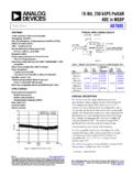
1 18-Bit, 1 MSPS PulSAR 7 mW ADC in MSOP/LFCSP . data sheet ad7982 . FEATURES FUNCTIONAL BLOCK DIAGRAM. 18-bit resolution with no missing codes TO 5V Throughput: 1 MSPS. Low power dissipation 4 mW at 1 MSPS (VDD only) REF VDD VIO TO 5V. IN+ SDI. 7 mW at 1 MSPS (total) 3- OR 4-WIRE. ad7982 SCK INTERFACE. 70 W at 10 kSPS 10V, 5V, .. SDO (SPI, CS. IN . INL: 1 LSB typical, 2 LSB maximum GND CNV DAISY CHAIN). ADA4940-1/. 06513-001. Dynamic range: 99 dB typical ADA4941-1. True differential analog input range: VREF Figure 1. 0 V to VREF with VREF between V to V. Allows use of any input range GENERAL DESCRIPTION. Easy to drive with the ADA4941-1 or ADA4940-1 The ad7982 is an 18-bit, successive approximation, analog-to- No pipeline delay digital converter (ADC) that operates from a single power supply, Single-supply V operation with V, V, 3 V, and 5 V VDD. The ad7982 contains a low power, high speed, 18-bit logic interface sampling ADC and a versatile serial interface port.
2 On the CNV. Proprietary serial interface SPI-/QSPI / MICROWIRE -/ rising edge, the ad7982 samples the voltage difference between DSP-compatible1 the IN+ and IN pins. The voltages on these pins usually swing Ability to daisy-chain multiple ADCs and busy indicator in opposite phases between 0 V and VREF. The reference voltage, 10-Lead msop and 3 mm 3 mm 10-Lead lfcsp VREF, is applied externally and can be set independent of the supply voltage, VDD. Its power scales linearly with throughput. APPLICATIONS. Battery-powered equipment The serial peripheral interface (SPI)-compatible serial interface data acquisition systems also features the ability, using the SDI input, to daisy-chain Medical instruments several ADCs on a single 3-wire bus and provides an optional Seismic data acquisition systems busy indicator. The ad7982 is compatible with V, V, 3 V, and 5 V logic, using the separate VIO supply. The ad7982 is available in a 10-lead msop or a 10-lead lfcsp .
3 With operation specified from 40 C to +85 C. Table 1. msop and lfcsp 14-/16-/18-Bit PulSAR ADCs 400 kSPS. Bits 100 kSPS 250 kSPS to 500 kSPS 1000 kSPS. 181 AD7989-1 AD7691 AD7690 ad7982 . AD7989-5 AD7984. 161 AD7684 AD7687 AD7688 AD7915. AD7693. AD7916. 162 AD7680 AD7685 AD7686 AD7980. AD7683 AD7694 AD7988-5 AD7983. AD7988-1. 142 AD7940 AD7942 AD7946. 1. True differential. 2. Pseudo differential. 1. Protected by Patent 6,703,961. Rev. D Document Feedback Information furnished by Analog Devices is believed to be accurate and reliable. However, no responsibility is assumed by Analog Devices for its use, nor for any infringements of patents or other rights of third parties that may result from its use. Specifications subject to change without notice. No One Technology Way, Box 9106, Norwood, MA 02062-9106, license is granted by implication or otherwise under any patent or patent rights of Analog Devices. Tel: 2007 2017 Analog Devices, Inc.
4 All rights reserved. Trademarks and registered trademarks are the property of their respective owners. Technical Support ad7982 data sheet TABLE OF CONTENTS. Features .. 1 Driver Amplifier Choice .. 15. Applications .. 1 Single-Ended to Differential 16. Functional Block Diagram .. 1 Voltage Reference Input .. 16. General Description .. 1 Power 16. Revision History .. 2 Digital Interface .. 17. 3 CS Mode, 3-Wire Without Busy Indicator .. 18. Timing Specifications .. 5 CS Mode, 3-Wire with Busy Indicator .. 19. Absolute Maximum 7 CS Mode, 4-Wire Without Busy Indicator .. 20. ESD Caution .. 7 CS Mode, 4-Wire with Busy Indicator .. 21. Pin Configurations and Function Descriptions .. 8 Chain Mode Without Busy Indicator .. 22. Typical Performance Characteristics .. 9 Chain Mode with Busy Indicator .. 23. Terminology .. 12 Applications Information .. 24. Theory of Operation .. 13 Layout .. 24. Circuit Information .. 13 Evaluating the Performance of the 24.
5 Converter Operation .. 13 Outline Dimensions .. 25. Typical Connection Diagram .. 14 Ordering Guide .. 25. Analog Inputs .. 15. REVISION HISTORY. 1/2017 Rev. C to Rev. D Added Patent Footnote ..1. Deleted QFN .. Throughout 7/2013 Rev. A to Rev. B. Changes to Features Section, Figure 1, and Table 1 .. 1 Added Low Power Dissipation of 4 mW at 1 MSPS (VDD only). Changed to VIO = V to V to VIO = V to V .. 3 to Features Section ..1. Changes to Table 2 .. 3 Changes to Power Dissipation; Table Deleted VIO Range Parameter, Table 3 .. 4 Added EPAD Notation to Figure 5 and Table 6 ..7. Changed to VIO = V to V to VIO = V to V .. 4 Updated Outline Dimensions .. 24. Changes to VIO Parameter, Table 3 .. 4 Changes to Ordering Guide .. 24. Changes to Table 4 .. 5. Added Table 5; Renumbered Sequentially .. 6 10/2007 Rev. 0 to Rev. A. Changes to Figure 5 and Table 7 .. 8 Changes to Table 1 and Layout ..1. Moved Typical Performance Characteristics Section.
6 9 Changes to Table Changes to Figure 9 .. 9 Changes to Layout ..5. Changes to Figure 23 .. 14 Changes to Layout ..6. Changes to Analog Inputs Section and Table 9 .. 15 Changes to Figure 5 ..7. Change to Single-Ended to Differential Driver Section Title .. 16 Changes to Figure 18 and Figure 11. Changes to Power Supply Section .. 16 Changes to Figure 13. Changes to Figure 30 .. 18 Changers to Figure 26 .. 15. Changes to Figure 32 .. 19 Changes to Digital Interface Section .. 16. Changes to Figure 34 .. 20 Changes to Figure 21. Changes to Figure 36 .. 21 Changes to Figure 22. Changes to Chain Mode with Busy Indicator .. 23 Updated Outline Dimensions .. 24. Changes to Applications Information 24 Changes to Ordering Guide .. 24. Changes to Ordering Guide .. 25. 3/2007 Revision 0: Initial Version 6/2014 Rev. B to Rev. C. Rev. D | Page 2 of 25. data sheet ad7982 . SPECIFICATIONS. VDD = V, VIO = V to V, VREF = 5 V, TA = 40 C to +85 C, unless otherwise noted.
7 Table 2. Parameter Test Conditions/Comments Min Typ Max Unit RESOLUTION 18 Bits ANALOG INPUT. Voltage Range IN+ IN VREF +VREF V. Absolute Input Voltage IN+ and IN VREF + V. Common-Mode Input Range IN+ and IN VREF VREF VREF V. Analog Input Common Mode Rejection fIN = 450 kHz 67 dB. Ratio (CMRR). Leakage Current at 25 C Acquisition phase 200 nA. Input Impedance See the Analog Inputs section ACCURACY. No Missing Codes 18 Bits Differential Linearity Error (DNL) + LSB1. Integral Linearity Error (INL) 2 1 +2 LSB1. Transition Noise VREF = 5 V LSB1. Gain Error, TMIN to TMAX2 + + % of FS. Gain Error Temperature Drift 1 ppm/ C. Zero Error, TMIN to TMAX2 100 +700 V. Zero Temperature Drift ppm/ C. Power Supply Rejection Ratio (PSRR) VDD = V 5% 90 dB. THROUGHPUT. Conversion Rate VIO V 0 1 MSPS. VIO V 0 800 kSPS. Transient Response Full-scale step 290 ns AC ACCURACY. Dynamic Range VREF = 5 V 97 99 dB3. VREF = V 93 dB3. Oversampled Dynamic Range4 FO = 1 kSPS 129 dB3.
8 Signal-to-Noise Ratio (SNR) fIN = 1 kHz, VREF = 5 V 98 dB3. fIN = 1 kHz, VREF = V dB3. Spurious-Free Dynamic Range (SFDR) fIN = 10 kHz 115 dB3. Total Harmonic Distortion5 (THD) fIN = 10 kHz 120 dB3. Signal-to-Noise-and-Distortion (SINAD) fIN = 1 kHz, VREF = 5 V 97 dB3. 1. LSB means least significant bit. With the 5 V input range, 1 LSB is V. 2. See Terminology section. These specifications include full temperature range variation but not the error contribution from the external reference. 3. All specifications expressed in decibels are referred to a full-scale input range (FSR )and tested with an input signal at dB below full scale, unless otherwise specified. 4. Dynamic range is obtained by oversampling the ADC running at a throughput FS of 1 MSPS followed by postdigital filtering with an output word rate of FO. 5. Tested fully in production at fIN = 1 kHz. Rev. D | Page 3 of 25. ad7982 data sheet VDD = V, VIO = V to V, VREF = 5 V, TA = 40 C to +85 C, unless otherwise noted.
9 Table 3. Parameter Test Conditions/Comments Min Typ Max Unit REFERENCE. Voltage Range V. Load Current 1 MSPS, VREF = 5 V 350 A. SAMPLING DYNAMICS. 3 dB Input Bandwidth 10 MHz Aperture Delay VDD = V 2 ns DIGITAL INPUTS. Logic Levels VIL VIO > 3 V + VIO V. VIH VIO > 3 V VIO VIO + V. VIL VIO 3 V + VIO V. VIH VIO 3 V VIO VIO + V. IIL 1 +1 A. IIH 1 +1 A. DIGITAL OUTPUTS. data Format Serial 18 bits, twos complement Pipeline Delay Conversion results available immediately after completed conversion VOL ISINK = +500 A V. VOH ISOURCE = 500 A VIO V. POWER SUPPLIES. VDD V. VIO V. Standby Current1, 2 VDD and VIO = V, 25 C A. Power Dissipation VDD = V, VREF = 5 V, VIO = 3 V. Total 10 kSPS throughput 70 86 W. 1 MSPS throughput 7 mW. VDD Only 4 mW. REF Only mW. VIO Only mW. Energy per Conversion nJ/sample TEMPERATURE RANGE3. Specified Performance TMIN to TMAX 40 +85 C. 1. With all digital inputs forced to VIO or GND as required. 2. During acquisition phase.
10 3. Contact an Analog Devices, Inc., sales representative for the extended temperature range. Rev. D | Page 4 of 25. data sheet ad7982 . TIMING SPECIFICATIONS. VDD = V to V, VIO = V to V, TA = 40 C to +85 C, unless otherwise Table 4. Parameter Symbol Min Typ Max Unit CONVERSION AND ACQUISTION TIMES. Conversion Time: CNV Rising Edge to data Available tCONV 500 710 ns Acquisition Time tACQ 290 ns Time Between Conversions tCYC 1000 ns CNV PULSE WIDTH (CS MODE) tCNVH 10 ns SCK. SCK Period (CS Mode) tSCK. VIO Above V ns VIO Above 3 V 12 ns VIO Above V 13 ns VIO Above V 15 ns SCK Period (Chain Mode) tSCK. VIO Above V ns VIO Above 3 V 13 ns VIO Above V 14 ns VIO Above V 16 ns SCK Low Time tSCKL ns SCK High Time tSCKH ns SCK Falling Edge to data Remains Valid tHSDO 3 ns SCK Falling Edge to data Valid Delay tDSDO. VIO Above V ns VIO Above 3 V 11 ns VIO Above V 12 ns VIO Above V 14 ns CS MODE. CNV or SDI Low to SDO D17 MSB Valid tEN. VIO Above 3 V 10 ns VIO Above V 15 ns CNV or SDI High or Last SCK Falling Edge to SDO High Impedance tDIS 20 ns SDI Valid Setup Time from CNV Rising Edge tSSDICNV 5 ns SDI Valid Hold Time from CNV Rising Edge tHSDICNV 2 ns CHAIN MODE.