Transcription of 2.4 GHz Low-Power RF Transceiver (Rev. A - TI.com
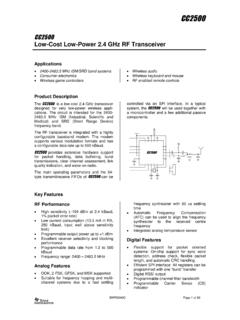
1 CC2400. CC2400. GHz Low-Power RF Transceiver Applications GHz MHz ISM/SRD band systems Wireless audio Game controllers PC peripherals Sports and leisure equipment Advanced toys Product Description The CC2400 is a true single-chip GHz and error detection reducing the workload RF Transceiver designed for Low-Power on the host microcontroller. and low-voltage wireless applications. The RF Transceiver is integrated with a The main operating parameters of CC2400. baseband modem supporting data rates can be programmed via an SPI-bus. In a up to 1 Mbps. typical system CC2400 will be used together with a microcontroller and a few The CC2400 is a low-cost, highly integrated external, passive components. solution enabling robust wireless communication in the - GHz CC2400 is based on Chipcon's SmartRF - unlicensed ISM band. It is intended for 03 technology in m CMOS. systems compliant with world-wide regulations covered by EN 300 440. (Europe), CFR47 Part 15 (US) and ARIB. STD-T66 (Japan).
2 Targeting a wide range of applications at GHz, the CC2400 supports over-the-air data rates of 10 kbps, 250 kbps and 1 Mbps without requiring any modifications to the hardware. The CC2400 provides extensive hardware support for packet handling, data buffering, burst transmissions, data coding Key Features True single-chip GHz RF Packet handling hardware Transceiver with baseband modem Data buffering 10 kbps, 250 kbps and 1 Mbps over- Digital RSSI output the-air data rates Small size (QFN 48 package), 7x7 mm Low current consumption (RX: 24 mA) Reference design complies with EN. Low core supply voltage ( V) 300 328, EN 300 440, FCC CFR47 part Programmable output power 15 and ARIB STD-T66. No external RF switch / filter needed Powerful and flexible development I/Q low-IF receiver tools available I/Q direct up-conversion transmitter Easy-to-use software for generating the Few external components CC2400 configuration data FIFO allows bursting of data This document contains information on a pre-production product.
3 Specifications and information herein are subject to change without notice. SWRS042A Page 1 of 83. CC2400. Table of contents 1 4. 2 FEATURES .. 5. 3 ABSOLUTE MAXIMUM 6. 4 OPERATING CONDITIONS .. 6. 5 ELECTRICAL SPECIFICATIONS .. 7. 6 GENERAL CHARACTERISTICS .. 7. 7 RF TRANSMIT SECTION .. 8. 8 RF RECEIVE 9. 9 AFC SECTION .. 10. 10 RSSI / CARRIER SENSE 11. 11 IF 11. 12 FREQUENCY SYNTHESIZER 11. 13 DIGITAL 12. 14 PIN 13. 15 CIRCUIT DESCRIPTION .. 15. 16 APPLICATION 17. INPUT / OUTPUT MATCHING .. 17. BIAS RESISTOR .. 17. CRYSTAL .. 17. DIGITAL I/O .. 17. POWER SUPPLY DECOUPLING AND FILTERING .. 17. POWER SUPPLY SWITCHING .. 17. 17 CONFIGURATION 20. 18 CONFIGURATION 20. 19 4-WIRE SERIAL CONFIGURATION 21. 20 OVERVIEW OF CONFIGURATIONS AND HARDWARE SUPPORT .. 24. 21 MICROCONTROLLER INTERFACE AND PIN CONFIGURATION .. 25. CONFIGURATION INTERFACE .. 25. SIGNAL INTERFACE IN UN-BUFFERED 25. GENERAL CONTROL AND STATUS PINS .. 25. 22 DATA 27. BUFFERED MODE .. 27. BUFFERED MODE HARDWARE SUPPORT.
4 27. 23 PACKET HANDLING HARDWARE 29. DATA PACKET FORMAT .. 29. ERROR DETECTION .. 29. HARDWARE INTERFACE .. 31. 24 DATA / LINE ENCODING .. 31. DATA ENCODING IN BUFFERED 31. DATA ENCODING IN UN-BUFFERED MODE .. 32. 25 RADIO CONTROL STATE MACHINE .. 34. 26 POWER MANAGEMENT FLOW CHART .. 36. 27 FSK MODULATION FORMATS .. 38. 28 BUILT-IN TEST PATTERN 38. 29 RECEIVER CHANNEL BANDWIDTH .. 39. 30 DATA RATE 40. 31 DEMODULATOR, BIT SYNCHRONIZER AND DATA DECISION .. 41. 32 AUTOMATIC FREQUENCY CONTROL .. 42. 33 LINEAR IF AND AGC SETTINGS .. 43. 34 44. 35 CARRIER SENSE .. 45. 36 INTERFACING AN EXTERNAL LNA OR PA .. 45. 37 GENERAL PURPOSE / TEST OUTPUT CONTROL PINS .. 45. 38 FREQUENCY 47. TRANSMIT MODE .. 47. SWRS042A Page 2 of 83. CC2400. RECEIVE MODE .. 47. 39 ALTERNATE TX IF SETTING .. 47. 40 VCO .. 48. 41 VCO 48. 42 OUTPUT POWER PROGRAMMING .. 48. 43 CRYSTAL OSCILLATOR .. 49. 44 INPUT / OUTPUT 50. 45 TYPICAL PERFORMANCE 50. 46 SYSTEM CONSIDERATIONS AND GUIDELINES .. 53. SRD 53. FREQUENCY HOPPING AND MULTI-CHANNEL SYSTEMS.
5 53. DATA BURST TRANSMISSIONS .. 53. CONTINUOUS TRANSMISSIONS .. 53. CRYSTAL DRIFT COMPENSATION .. 53. SPECTRUM EFFICIENT MODULATION .. 54. LOW LATENCY SYSTEMS .. 54. LOW COST SYSTEMS .. 54. BATTERY OPERATED SYSTEMS .. 54. INCREASING OUTPUT POWER .. 54. 47 PCB LAYOUT RECOMMENDATIONS .. 56. 48 ANTENNA CONSIDERATIONS .. 57. 49 CONFIGURATION REGISTERS .. 58. 50 PACKAGE DESCRIPTION (QFN48) .. 76. 51 RECOMMENDED LAYOUT FOR PACKAGE (/QFN48).. 77. 52 PACKAGE THERMAL 77. 53 SOLDERING 77. 54 IC MARKING .. 78. 55 PLASTIC TUBE 80. 56 CARRIER TAPE AND REEL SPECIFICATION .. 80. 57 ORDERING 80. 58 GENERAL 81. DOCUMENT HISTORY .. 81. PRODUCT STATUS DEFINITIONS .. 82. 82. TRADEMARKS .. 82. LIFE SUPPORT POLICY .. 82. 59 ADDRESS 83. SWRS042A Page 3 of 83. CC2400. 1 Abbreviations ACP Adjacent Channel Power ACR Adjacent Channel Rejection ADC Analog-to-Digital Converter AFC Automatic Frequency Correction AGC Automatic Gain Control BER Bit Error Rate BOM Bill Of Materials bps bits per second BT Bandwidth-Time product (for GFSK).
6 CRC Cyclic Redundancy Check CSMA Carrier Sense Multiple Access CSMA / CA Carrier Sense Multiple Access / Collision Avoidance DAC Digital-to-Analog Converter ESR Equivalent Series Resistance FH Frequency Hopping FHSS Frequency Hopping Spread Spectrum FIFO First In First Out (queue). FS Frequency Synthesizer FSK Frequency Shift Keying GFSK Gaussian Frequency Shift Keying IF Intermediate Frequency ISM Industrial Scientific Medical kbps kilo bits per second LNA Low Noise Amplifier Mbps Mega bits per second MCU Micro Controller Unit NRZ Non Return to Zero PA Power Amplifier PD Phase Detector PCB Printed Circuit Board PN9 Pseudo-random Bit Sequence (9-bit). PLL Phase Locked Loop PRN Pseudo Random Number PRNG Pseudo Random Number Generator RF Radio Frequency RSSI Received Signal Strength Indicator RX Receive (mode). SPI Serial Peripheral Interface SRD Short Range Device TBD To Be Decided/Defined TDMA Time Division Multiple Access TX Transmit (mode). VCO Voltage Controlled Oscillator VGA Variable Gain Amplifier SWRS042A Page 4 of 83.
7 CC2400. 2 Features 2400 2483 MHz RF Transceiver GFSK and FSK modulation Packet handling hardware support Very low current consumption (RX: Preamble generator with 24 mA) programmable length Over-the-air data rates of 10 kbps, Programmable synchronization 250 kbps and 1 Mbps word insertion/detection High sensitivity (-87 dBm @ 1 Mbps, CRC computation over the data BER=10-3) field Agile frequency synthesizer (40 us 8B/10B line coding option settling time). On-chip VCO, LNA and PA Data buffering Low core supply voltage ( V) 32 byte FIFO. Flexible I/O supply voltage Provides for flexible communication ( V) to match the signal with the host controller. levels of the interfacing Burst transmission reduces the microcontroller average power consumption. Programmable output power I/Q low-IF receiver Powerful and flexible development I/Q direct up-conversion transmitter tools available Fully equipped development kit Few external components Demonstration board reference Only reference crystal and a few design with microcontroller code passives needed Easy-to-use SmartRF Studio No external filters needed software for generating the CC2400.
8 Configuration data Programmable baseband modem 4-wire SPI interface Small size (QFN 48 package) 7 x 7 mm Serial clock up to 20 MHz Digital RSSI output Reference design complies with EN. 300 328, EN 300 440, FCC CFR47 part 15 and ARIB STD-T66. SWRS042A Page 5 of 83. CC2400. 3 Absolute Maximum Ratings Parameter Min. Max. Units Condition Supply voltage, chip core, V. Supply voltage ( ), digital I/O V. Voltage on any pin, core VDD+ , V. max Voltage on any pin, digital I/O (pin no. 27-35) VDDIO+ , V. max Input RF level 10 dBm Storage temperature range 50 150 C. Reflow solder temperature 260 C T = 10 s NOTE: The supply voltage to the chip core ( ) should not be switched off when the digital IO ( ). supply voltage is still applied to the chip. If this is done, a large current will flow inside the CC2400 and the chip may be damaged as a result. If the core supply needs to be switched off to lower the power consumption, please see page 17 for a suggested solution. The absolute maximum ratings given the limiting values may cause permanent above should under no circumstances be damage to the device.
9 Violated. Stress exceeding one or more of Caution! ESD sensitive device. Precaution should be used when handling the device in order to prevent permanent damage. 4 Operating Conditions Parameter Min. Typ. Max. Unit Condition Supply voltage, chip core, V. Supply voltage ( ), digital V The digital I/O voltage ( I/O, VDDIO pin) must match the interfacing circuit. Recommended supply voltage, chip core, Recommended supply voltage ( ), digital I/O Operating ambient temperature 40 85 C. range SWRS042A Page 6 of 83. CC2400. 5 Electrical Specifications Parameter Min. Typ. Max. Unit Condition / Note Current Consumption, Power Down mode (OFF) 5 A Oscillator core off Current Consumption, Idle mode (IDLE) mA. Current Consumption, Frequency synthesizer (FS_ON) mA. Current Consumption, 24 mA. Receive mode Current Consumption, Transmit mode: P= 25 dBm 11 mA The output power is delivered differentially to a 50 single- P= 5 dBm 15 mA ended load through a balun, see also p. 50. P=0 dBm 19 mA.
10 Current Consumption, crystal 38 A 16 MHz, 16 pF load crystal oscillator core Table 1 Electrical specifications 6 General Characteristics Tc = 25 C, = V, = (digital I/O) if nothing else stated. Measured on Chipcon's CC2400EM reference design. Parameter Min. Typ. Max. Unit Condition / Note RF Frequency Range 2400 2483 MHz Programmable in 1 MHz channel steps. Data rate 10 kbps Data rate is 250 kbps programmable/selectable, see 1 Mbps page 40. Table 2 General characteristics SWRS042A Page 7 of 83. CC2400. 7 RF Transmit section Tc = 25 C, = V, = (digital I/O) if nothing else stated. Measured on Chipcon's CC2400EM reference design. Parameter Min. Typ. Max. Unit Condition / Note Binary FSK frequency deviation 0 250 500 kHz The frequency corresponding to the digital "0" is denoted f0, while f1 corresponds to a digital "1". The frequency deviation is given by fd= (f1 f0)/2. The RF carrier frequency, fc, is then given by fc=(f0+f1)/2. Nominal output power 0 dBm Default settings. Power delivered to a 50 single- ended load through a balun.
