Transcription of 200A, 30V N-CHANNEL POWER MOSFET - Unisonic
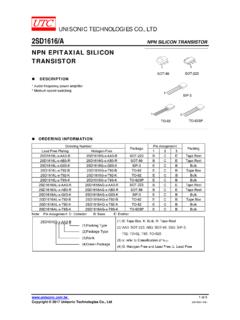
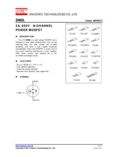
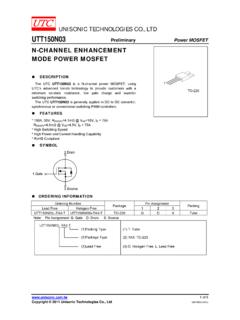
1 Unisonic TECHNOLOGIES CO., LTD UTT200N03 POWER MOSFET 1 of 6 Copyright 2017 Unisonic Technologies Co., Ltd 200a , 30V N-CHANNEL POWER MOSFET DESCRIPTION The UTC UTT200N03 is a N-CHANNEL MOSFET using UTC s advanced technology to provide customers with a minimum on-state resistance and superior switching performance. The UTC UTT200N03 is generally applied in DC to DC convertor or synchronous rectification FEATURES * Fast Switching * 100% Avalanche Tested * High POWER and Current Handling Capability * RoHS Compliant SYMBOL ORDERING INFORMATION Ordering Number Pin Assignment Lead Free Halogen Free Package 1 2 3 Packing UTT200N03L-TA3-T UTT200N03G-TA3-T TO-220 G D S Tube UTT200N03L-TQ2-T UTT200N03G-TQ2-T TO-263 G D S Tube UTT200N03L-TQ2-R UTT200N03G-TQ2-R TO-263 G D S Tape ReelNote: Pin Assignment: G: Gate D: Drain S.
2 Source MARKING UTT200N03 POWER MOSFET Unisonic TECHNOLOGIES CO., LTD 2 of 6 ABSOLUTE MAXIMUM RATINGS [TC=25 C, unless otherwise specified (Note 6)] PARAMETER SYMBOL RATINGS UNIT Drain-Source Voltage VDSS 30 V Gate-Source Voltage VGSS 20 V Continuous ID 200 A Drain Current Pulsed (Note 2) IDM 800 A Single Pulsed Avalanche Energy (Note 3)
3 EAS 864 mJ Peak Diode Recovery dv/dt (Note 4) dv/dt V/ns POWER Dissipation TC=25 C 178 W POWER Dissipation Derate above 25 C PD W/ C Junction Temperature TJ -55 ~ +150 C Storage Temperature TSTG -55 ~ +150 C Notes: 1. Absolute maximum ratings are those values beyond which the device could be permanently damaged. Absolute maximum ratings are stress ratings only and functional device operation is not implied. 2. Repetitive Rating : Pulse width limited by maximum junction temperature. 3. L= , IAS=24A, VDD=30V, RG=25 , Starting TJ = 25 C 4.
4 ISD 30A, di/dt 200a / s, VDD BVDSS, Starting TJ = 25 C THERMAL CHARACTERISTICS PARAMETER SYMBOL RATINGS UNIT Junction to Ambient JA C/W Junction to Case JC C/W ELECTRICAL CHARACTERISTICS (TC=25 C, unless otherwise specified PARAMETER SYMBOL TEST CONDITIONS MIN TYP MAX UNITOFF CHARACTERISTICS Drain-Source Breakdown Voltage BVDSS ID=250 A, VGS=0V 30 V Drain-Source Leakage Current IDSS VDS=30V, VGS=0V 10 AForward VGS=+20V, VDS=0V +100nAGate- Source Leakage Current Reverse IGSS VGS=-20V, VDS=0V -100nAON CHARACTERISTICS Gate Threshold Voltage VGS(TH) VDS=VGS, ID=250 A Static Drain-Source On-State Resistance RDS(ON))
5 VGS=10V, ID=80A DYNAMIC PARAMETERS Input Capacitance CISS 5490 7300pFOutput Capacitance COSS 1220 1620pFReverse Transfer Capacitance CRSS VGS=0V, VDS=25V, f= 155 233pFSWITCHING PARAMETERS Total Gate Charge QG 200 350nCGate to Source Charge QGS 11 nCGate to Drain Charge QGD VGS=10V, VDS=25V, ID=100A 40 nCTurn-ON Delay Time tD(ON)
6 70 110nsRise Time tR 200 300nsTurn-OFF Delay Time tD(OFF) 1600 2000nsFall-Time tF VDD=30V, ID= , RGEN= , VGS=10V 700 1200nsSOURCE- DRAIN DIODE RATINGS AND CHARACTERISTICS Maximum Body-Diode Continuous Current IS 200a Maximum Body-Diode Pulsed Current ISM 800A Drain-Source Diode Forward Voltage VSD IS=100A.
7 VGS=0V Reverse Recovery Time trr 185 nsReverse Recovery Charge Qrr IS=30A,VGS=0V, dI/dt=100A/ s 500 nCUTT200N03 POWER MOSFET Unisonic TECHNOLOGIES CO., LTD 3 of 6 TEST CIRCUITS AND WAVEFORMS VDS+-DUTRGdv/dt controlled by RGISD controlled by pulse periodVDDPeak Diode Recovery dv/dt Test Circuit & WaveformsSame Type as DUTISDVGSLVGS(Driver)ISD(DUT)VDS(DUT)D=G ate Pulse WidthGate Pulse Period10 Vdi/dtBody Diode Reverse CurrentIRMBody Diode Recovery dv/dtVDDVSDBody Diode Forward Voltage DropIFM, Body Diode Forward CurrentDriver UTT200N03 POWER MOSFET Unisonic TECHNOLOGIES CO.
8 , LTD 4 of 6 TEST CIRCUITS AND WAVEFORMS DUTVDS10 VChargeQGSQGDQGGate Charge Test CircuitGate Charge WaveformsVGSVGS1mARL 10 VtPRGDUTLVDSIDVDDU nclamped Inductive Switching Test CircuittPVDDIASBVDSSID(t)VDS(t)TimeEAS=2 1 LIAS2 BVDSSBVDSS-VDDU nclamped Inductive Switching Waveforms UTT200N03 POWER MOSFET Unisonic TECHNOLOGIES CO., LTD 5 of 6 TYPICAL CHARACTERISTICS UTT200N03 POWER MOSFET Unisonic TECHNOLOGIES CO., LTD 6 of 6 UTC assumes no responsibility for equipment failures that result from using products at values that exceed, even momentarily, rated values (such as maximum ratings, operating condition ranges, or other parameters) listed in products specifications of any and all UTC products described or contained herein.
9 UTC products are not designed for use in life support appliances, devices or systems where malfunction of these products can be reasonably expected to result in personal injury. Reproduction in whole or in part is prohibited without the prior written consent of the copyright owner. UTC reserves the right to make changes to information published in this document, including without limitation specifications and product descriptions, at any time and without notice. This document supersedes and replaces all information supplied prior to the publication hereof.