Transcription of 25 MHz to 3000 MHz Fractional-N PLL with Integrated VCO ...
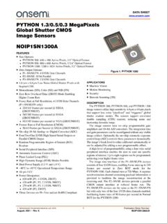
1 25 MHz to 3000 MHz Fractional-N PLL with Integrated VCO. Data Sheet HMC832A. FEATURES FUNCTIONAL BLOCK DIAGRAM. LD/SDO SCK SDI. RF bandwidth: 25 MHz to 3000 MHz V supply HMC832A LOCK. DETECT. Maximum phase detector rate: 100 MHz Ultralow phase noise CONTROL. SPI. PROGRAMMING SEN. INTERFACE. 110 dBc/Hz in band (typical), fO at 1600 MHz EN. Fractional figure of merit (FOM): 226 dBc/Hz MODULATOR CAL RF_P. 24-bit step size, 3 Hz typical resolution Exact frequency mode with 0 Hz frequency error EN RF_N. Fast frequency hopping 1, 2, 4, 6, ..62. 40-lead, 6 mm 6 mm LFCSP package: 36 mm2. N. APPLICATIONS VCO. CP CP PFD VTUNE.
2 Cellular infrastructure Microwave radios R. WiMax, WiFi 13110-001. Communications test equipment XREFP. CATV equipment Figure 1. DDS replacement Military Tunable reference sources for spurious-free performance GENERAL DESCRIPTION. The HMC832A is a V, high performance, wideband, frac- The HMC832A is footprint compatible to the HMC830 PLL. tional-N, phase- locked loop (PLL) that features an Integrated with an Integrated VCO. It features V supply and innovative voltage controlled oscillator (VCO) with a fundamental programmable performance technology that enables the frequency of 1500 MHz to 3000 MHz and an Integrated VCO HMC832A to tailor current consumption and corresponding output divider (divide by 1, 2, 4, 6, 62) that enables the noise floor performance to individual applications by selecting HMC832A to generate continuous frequencies from 25 MHz to either a low current consumption mode or a high performance 3000 MHz.
3 The Integrated phase detector (PD) and - mode for improved noise floor performance. modulator, capable of operating at up to 100 MHz, permit wider Additional features of the HMC832A include 12 dB of RF. loop bandwidths and faster frequency tuning with excellent output gain control in 1 dB steps; an output mute function to spectral performance. automatically mute the output during frequency changes when Industry leading phase noise and spurious performance, across the device is not locked ; selectable output return loss;. all frequencies, enable the HMC832A to minimize blocker programmable differential or single-ended outputs, with the effects, and to improve receiver sensitivity and transmitter ability to select either output in single-ended mode; a.
4 Spectral purity. A low noise floor ( 160 dBc/Hz eliminates any modulator exact frequency mode that enables users to generate contribution to modulator/mixer noise floor in transmitter output frequencies with 0 Hz frequency error; and a register applications. configurable V or V serial port interface (SPI). Rev. B Document Feedback Information furnished by Analog Devices is believed to be accurate and reliable. However, no responsibility is assumed by Analog Devices for its use, nor for any infringements of patents or other rights of third parties that may result from its use. Specifications subject to change without notice.)
5 No One Technology Way, Box 9106, Norwood, MA 02062-9106, license is granted by implication or otherwise under any patent or patent rights of Analog Devices. Tel: 2015 Analog Devices, Inc. All rights reserved. Trademarks and registered trademarks are the property of their respective owners. Technical Support HMC832A Data Sheet TABLE OF CONTENTS. Features .. 1 ID, Read Address, and Reset (RST) Registers .. 35. Applications .. 1 Reference Divider (REFDIV), Integer, and Fractional Functional Block Diagram .. 1 Frequency Registers .. 35. General Description .. 1 VCO SPI Register .. 36. Revision History .. 2 - Configuration Register.
6 36. 3 Lock Detect Register .. 37. Timing Specifications .. 6 Analog Enable (EN) Register .. 37. Absolute Maximum Ratings .. 7 Charge Pump Register .. 38. Recommended Operating Conditions .. 7 Autocalibration 38. ESD Caution .. 7 Phase Detector (PD) Register .. 39. Pin Configuration and Function Descriptions .. 8 Exact Frequency Mode Register .. 39. Typical Performance Characteristics .. 9 General-Purpose, SPI, and Reference Divider (GPO_SPI_RDIV) Register .. 40. Theory of Operation .. 15. VCO Tune Register .. 41. PLL Subsystem Overview .. 15. Sucessive Approximation Register .. 41. VCO Subsystem Overview.
7 15. General-Purpose 2 Register .. 41. SPI Configuration of PLL and VCO Subsystems .. 15. Built-In Self Test (BIST) Register .. 41. VCO Subsystem .. 17. VCO Subsystem Register Map .. 42. PLL Subsystem .. 21. VCO Enable Register .. 42. Soft Reset and Power-On Reset .. 28. VCO Output Divider Register .. 43. Power-Down Mode .. 28. VCO Configuration Register .. 43. General-Purpose Output (GPO) .. 28. VCO Calibration/Bias, Center Frequency Calibration Chip Identification .. 29 (CF_CAL), and MSB Calibration Registers .. 44. Serial Port Interface (SPI) .. 29 VCO Output Power Control .. 44. Applications Information.
8 32 Evaluation Printed Circuit Board (PCB) .. 45. Power Supply .. 33 Changing Evaluation Board Reference Frequency and CP. Programmable Performance 33 Current Configuration .. 46. Loop Filter and Frequency Changes .. 33 Evaluation Kit Contents .. 46. RF Programmable Output Return 34 Outline Dimensions .. 47. Mute Mode .. 34 Ordering Guide .. 48. PLL Register Map .. 35. REVISION HISTORY. 11/15 Revision B: Initial Version Rev. B | Page 2 of 48. Data Sheet HMC832A. SPECIFICATIONS. VPPCP, VDDLS, VCC1, VCC2, RVDD, AVDD, DVDD, VCCPD, VCCHF, VCCPS = V minimum and maximum specified across the temperature range of 40 C to +85 C.
9 Table 1. Parameter Test Conditions/Comments Min Typ Max Unit RF OUTPUT CHARACTERISTICS. Output Frequency 25 3000 MHz VCO Frequency at PLL Input 1500 3000 MHz RF Output Frequency at fVCO 1500 3000 MHz OUTPUT POWER. RF Output Power Across all frequencies (see Figure 25), high performance mode (VCO_REG 0x03[1:0] = 3d). Maximum gain setting (VCO_REG 0x07[3:0] = 7 dBm 0xB), single-ended Gain Setting 6 (VCO_REG 0x07[3:0] = 6d), 2 dBm differential Output Power Control Range 1 dB steps 12 dB. HARMONICS FOR FUNDAMENTAL MODE. fO Mode at 2 GHz Second/third/fourth harmonics 20/ 29/ 45 dBc fO/2 Mode at 2 GHz/2 = 1 GHz Second/third/fourth harmonics 26/ 10/ 34 dBc fO/30 Mode at 3 GHz/30 = 100 MHz Second/third/fourth harmonics 33/ 10/ 40 dBc fO/62 Mode at 1550 MHz/62 = 25 MHz Second/third/fourth harmonics 40/ 6/ 43 dBc VCO OUTPUT DIVIDER.
10 VCO RF Divider Range 1, 2, 4, 6, 8, 62 1 62. PLL RF DIVIDER CHARACTERISTICS. 19-Bit N-Divider Range (Integer) Maximum = 219 1 16 524,287. 19-Bit N-Divider Range (Fractional) Fractional nominal divide ratio varies ( 4) 20 524,283. dynamically maximum REFERENCE (XREFP PIN) INPUT. CHARACTERISTICS. Maximum XREFP Input Frequency 350 MHz XREFP Input Level AC-coupled1 6 +12 dBm XREFP Input Capacitance 5 pF. 14-Bit R-Divider Range 1 16,383. PHASE DETECTOR (PD)2. PD Frequency Fractional Mode3 DC 100 MHz PD Frequency Integer Mode DC 100 MHz CHARGE PUMP. Output Current mA. Charge Pump Gain Step Size 20 A. PD/Charge Pump Single Sideband (SSB) 50 MHz reference, input referred Phase Noise 1 kHz 143 dBc/Hz 10 kHz Add 2 dB for fractional mode 150 dBc/Hz 100 kHz Add 3 dB for fractional mode 152 dBc/Hz LOGIC INPUTS V and V modes Input Voltage Low (VIL) V.