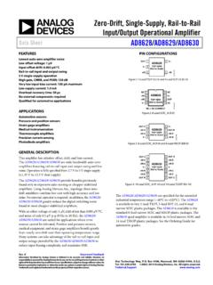
Transcription of –28 V, −200 mA, Low Noise, Linear Regulator Data Sheet …
1 28 V, 200 mA, Low Noise, Linear RegulatorData Sheet ADP7182 Rev. L Document Feedback Information furnished by Analog Devices is believed to be accurate and reliable. However, no responsibility is assumed by Analog Devices for its use, nor for any infringements of patents or other rights of third parties that may result from its use. Specifications subject to change without notice. No license is granted by implication or otherwise under any patent or patent rights of Analog Devices. Trademarks and registered trademarks are the property of their respective owners. One Technology Way, Box 9106, Norwood, MA 02062-9106, : 2013 2018 Analog Devices, Inc.
2 All rights reserved. Technical Support FEATURES Low noise: 18 V rms Power supply rejection ratio (PSRR): 66 dB at 10 kHz at VOUT = 3 V Positive or negative enable logic Stable with small F ceramic output capacitor Input voltage range: V to 28 V Maximum output current: 200 mA Low dropout voltage: 185 mV at 200 mA load Initial accuracy: 1% Accuracy over line, load, and temperature +2% maximum/ 3% minimum Low quiescent current, IGND = 650 A with 200 mA load Low shutdown current: 2 A Adjustable output from V to VIN + VDO Current-limit and thermal overload protection 6- and 8-lead LFCSP and 5-lead TSOT Supported by ADIsimPower tool APPLICATIONS Regulation to noise sensitive applications Analog-to-digital converter (ADC) and digital-to-analog converter (DAC) circuits, precision amplifiers Communications and infrastructure Medical and healthcare Industrial and instrumentation TYPICAL APPLICATION CIRCUITS GNDENNCVINVOUTADP7182 ONON 2 VOFF0V2 VVIN = 8 VVOUT = F10703-001 Figure 1.
3 ADP7182 with Fixed Output Voltage, VOUT = 5 V 13k GNDENADJVINVOUTADP7182 ONON 2 VOFF0V2 VVIN = 8 VVOUT = F10703-002 Figure 2. ADP7182 with Adjustable Output Voltage, VOUT = 5 V GENERAL DESCRIPTION The ADP7182 is a cmos , low dropout (LDO) Linear Regulator that operates from V to 28 V and provides up to 200 mA of output current. This high input voltage LDO is ideal for regu-lation of high performance analog and mixed signal circuits operating from 27 V down to V rails. Using an advanced proprietary architecture, it provides high power supply rejection and low noise, and achieves excellent line and load transient response with a small F ceramic output capacitor.
4 The ADP7182 is available in fixed output voltage and an adjustable version that allows the output voltage to range from V to VIN + VDO via an external feedback divider. The following fixed output voltages are available from stock: 5 V (3 mm 3 mm LFCSP), V, V, 3 V, 5 V (TSOT), V, V, V, 5 V ( mm mm LFCSP). Additional voltages are available by special order. The ADP7182 Regulator output noise is 18 V rms independent of the output voltage. The enable logic is capable of interfacing with positive or negative logic levels for maximum flexibility. The ADP7182 is available in 5-lead TSOT, 6- and 8-lead LFCSP packages for a small, low profile footprint.
5 ADP7182 Data Sheet Rev. L | Page 2 of 32 TABLE OF CONTENTS Features .. 1 Applications .. 1 Typical Application Circuits .. 1 General Description .. 1 Revision History .. 2 Specifications .. 4 Input and Output Capacitance, Recommended Specifications .. 5 Absolute Maximum Ratings .. 6 Thermal Data .. 6 Thermal Resistance .. 6 ESD Caution .. 6 Pin Configurations and Function Descriptions .. 7 Typical Performance Characteristics .. 10 Theory of Operation .. 22 Adjustable Mode Operation .. 22 Applications Information .. 23 ADIsimPower Design Tool .. 23 Capacitor Selection .. 23 Enable Pin Operation .. 24 Soft Start .. 24 Noise Reduction of the Adjustable ADP7182.
6 25 Current-Limit and Thermal Overload Protection .. 25 Thermal Considerations .. 26 PCB Layout Considerations .. 29 Outline Dimensions .. 31 Ordering Guide .. 32 REVISION HISTORY 10/2018 Rev. K to Rev. L Changes to Noise Reduction of the Adjustable ADP7182 Section .. 25 Changes to Ordering Guide .. 32 7/2018 Rev. J to Rev. K Changes to Outline Dimensions .. 30 Changes to Ordering Guide .. 31 3/2017 Rev. I to Rev. J Changes to Specifications Section .. 3 Updated Outline Dimensions .. 30 Changes to Ordering Guide .. 31 12/2016 Rev. H to Rev. I Changes to Figure 77 .. 21 Moved Theory of Operation/Enable Pin Operation 23 Changes to Enable Pin Operation Section.
7 23 11/2016 Rev. G to Rev. H Change to Thermal Considerations Section .. 25 Updated Outline Dimensions .. 30 Changes to Ordering Guide .. 31 6/2016 Rev. F to Rev. G Changes to Figure 101 .. 28 3/2016 Rev. E to Rev. F Changes to Figure 62 .. 17 9/2014 Rev. D to Rev. E Changes to Features and General Description Sections .. 1 Changes to Figure 101 .. 28 Added Table 11 .. 29 Changes to Ordering Guide .. 31 7/2014 Rev. C to Rev. D Added 6-Lead LFCSP (Throughout) .. 1 Added 6-Lead LFCSP Thermal Resistance Parameters .. 5 Added Figure 7, Figure 8, and Table 7 .. 8 Added 6-Lead LFCSP JA Values to Table 8; Added 6-Lead LFCSP JB Value to Table 10.
8 25 Added Figure 92, Figure 93, and Figure 94 .. 26 Changes to Thermal Characterization Parameter, JB Section and Added Figure 99 .. 27 Added Figure 101 .. 28 Added Figure 104, Outline Dimensions .. 29 Changes to Ordering Guide .. 30 9/2013 Rev. B to Rev. C Changes to Ordering Guide .. 28 6/2013 Rev. A to Rev. B Changes to General Description .. 1 Updated Outline Dimensions .. 27 Changes to Ordering Guide .. 28 Data Sheet ADP7182 Rev. L | Page 3 of 32 5/2013 R e v. 0 to Rev. A Changed Start-Up Time VOUT = 5 V from 450 s to 550 s .. 3 Changes to Figure 9 and Figure 12 .. 8 Changes to Figure 13 .. 9 Changes to Figure 19 and Figure 22.
9 10 Changes to Figure 28 .. 11 Changes to Figure 31 and Figure 34 .. 12 Changes to Figure 37 and Figure 40 .. 13 Changes to Figure 43 .. 14 Added ADIsimPower Design Tool Section .. 21 4/ 2013 Revision 0: Initial Ve r s i o n ADP7182 Data Sheet Rev. L | Page 4 of 32 SPECIFICATIONS VIN = (VOUT V) or V (whichever is more negative), EN = VIN, IOUT = 10 mA, CIN = COUT = F, TJ = 40 C to +125 C for minimum/maximum specifications, TA = 25 C for typical specifications, unless otherwise noted. Table 1. Parameter Symbol Test Conditions/Comments Min Typ Max Unit INPUT VOLTAGE RANGE VIN 28 V OPERATING SUPPLY CURRENT IGND IOUT = 0 A 33 53 A IOUT = 10 mA 100 150 A IOUT = 200 mA 650 850 A SHUTDOWN CURRENT IGND-SD EN = GND 2 A EN = GND, VIN = V to 28 V 8 A OUTPUT VOLTAGE ACCURACY Fixed Output Voltage Accuracy VOUT IOUT = 10 mA, TA = 25 C 1 +1 % 1 mA < IOUT < 200 mA, VIN = (VOUT V) to 28 V 3 +2 % Adjustable Output Voltage Accuracy VADJ IOUT = 10 mA V 1 mA < IOUT < 200 mA, VIN = (VOUT V)
10 To 28 V V LINE REGULATION VOUT/ VIN VIN = (VOUT V) to 28 V + %/V LOAD REGULATION1 VOUT/ IOUT IOUT = 1 mA to 200 mA %/mA ADJ INPUT BIAS CURRENT ADJI- BIAS 1 mA < IOUT < 200 mA, VIN = (VOUT V) to 28 V 10 nA DROPOUT VOLTAGE2 VDO IOUT = 10 mA 25 70 mV IOUT = 50 mA 46 90 mV IOUT = 200 mA 185 360 mV S TA R T-UP TIME3 tS TA R T-UP VOUT = 5 V 550 s VOUT = V 375 s CURRENT-LIMIT THRESHOLD4 ILIMIT 230 350 500 mA THERMAL SHUTDOWN Thermal Shutdown Threshold TSSD TJ rising 150 C Thermal Shutdown Hysteresis TSSD-HYS 15 C EN THRESHOLD Positive Rise VEN-POS-RISE VOUT = off to on (positive) V Negative Rise VEN-NEG-RISE VOUT = off to on (negative) V Positive Fall VEN-POS-FA L L VOUT = on to off (positive)
