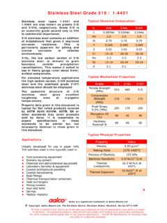
Transcription of 2N4401 General Purpose Transistors
1 Semiconductor Components Industries, LLC, 2010 February, 2010 Rev. 41 Publication Order Number: 2N4401 /D2N4401 General PurposeTransistorsNPN SiliconFeatures Pb Free Packages are Available*MAXIMUM RATINGSR atingSymbolValueUnitCollector Emitter VoltageVCEO40 VdcCollector Base VoltageVCBO60 VdcEmitter Base Current ContinuousIC600mAdcTotal Device Dissipation@ TA = 25 CDerate above 25 CTotal Device Dissipation@ TC = 25 CDerate above 25 COperating and Storage JunctionTemperature RangeTJ, Tstg 55 to+150 CTHERMAL CHARACTERISTICSC haracteristicSymbolMaxUnitThermal Resistance, Junction to AmbientRqJA200 C/WThermal Resistance, Junction to C/WStresses exceeding Maximum Ratings may damage the device. MaximumRatings are stress ratings only. Functional operation above the RecommendedOperating Conditions is not implied. Extended exposure to stresses above theRecommended Operating Conditions may affect device reliability.
2 *For additional information on our Pb Free strategy and soldering details, pleasedownload the ON Semiconductor Soldering and Mounting Techniques ReferenceManual, detailed ordering and shipping information in the packagedimensions section on page 2 of this data DIAGRAM2N4401 AYWWGG2N4401 = Device CodeA= Assembly LocationY= YearWW= Work WeekG= Pb Free Package(Note: Microdot may be in either location)12312 BENT LEADTAPE & REELAMMO PACKSTRAIGHT LEADBULK PACK3TO 92 CASE 29 STYLE 12N4401 CHARACTERISTICS (TA = 25 C unless otherwise noted)CharacteristicSymbolMinMaxUnitOFF CHARACTERISTICSC ollector Emitter Breakdown Voltage (Note 1)(IC = mAdc, IB = 0)V(BR)CEO40 VdcCollector Base Breakdown Voltage(IC = mAdc, IE = 0)V(BR)CBO60 VdcEmitter Base Breakdown Voltage(IE = mAdc, IC = 0)V(BR) VdcBase Cutoff Current(VCE = 35 Vdc, VEB = Vdc)IBEV Cutoff Current(VCE = 35 Vdc, VEB = Vdc)ICEX CHARACTERISTICS (Note 1)DC Current Gain(IC = mAdc, VCE = Vdc)(IC = mAdc, VCE = Vdc)(IC = 10 mAdc, VCE = Vdc)(IC = 150 mAdc, VCE = Vdc)(IC = 500 mAdc, VCE = Vdc)hFE20408010040 300 Collector Emitter Saturation Voltage(IC = 150 mAdc, IB = 15 mAdc)(IC = 500 mAdc, IB = 50 mAdc)VCE(sat)
3 Emitter Saturation Voltage(IC = 150 mAdc, IB = 15 mAdc)(IC = 500 mAdc, IB = 50 mAdc)VBE(sat) SIGNAL CHARACTERISTICSC urrent Gain Bandwidth Product(IC = 20 mAdc, VCE = 10 Vdc, f = 100 MHz)fT250 MHzCollector Base Capacitance(VCB = Vdc, IE = 0, f = MHz)Ccb Base Capacitance(VEB = Vdc, IC = 0, f = MHz)Ceb 30pFInput Impedance(IC = mAdc, VCE = 10 Vdc, f = kHz) WVoltage Feedback Ratio(IC = mAdc, VCE = 10 Vdc, f = kHz) 10 4 Small Signal Current Gain(IC = mAdc, VCE = 10 Vdc, f = kHz)hfe40500 Output Admittance(IC = mAdc, VCE = 10 Vdc, f = kHz) CHARACTERISTICSD elay Time(VCC = 30 Vdc, VBE = Vdc,IC = 150 mAdc, IB1 = 15 mAdc)td 15nsRise Timetr 20nsStorage Time(VCC = 30 Vdc, IC = 150 mAdc,IB1 = IB2 = 15 mAdc)ts 225nsFall Timetf 30ns1. Pulse Test: Pulse Width 300 ms, Duty Cycle INFORMATIOND evicePackageShipping 2N4401TO 925000 Units / Bulk2N4401 GTO 92(Pb Free)5000 Units / Bulk2N4401 RLRATO 922000 / Tape & Reel2N4401 RLRAGTO 92(Pb Free)2000 / Tape & Reel2N4401 RLRMGTO 92(Pb Free)2000 / Tape & Ammo Box2N4401 RLRPTO 922000 / Tape & Ammo Box2N4401 RLRPGTO 92(Pb Free)2000 / Tape & Ammo Box For information on tape and reel specifications, including part orientation and tape sizes, please refer to our Tape and Reel PackagingSpecifications Brochure, BRD8011 1.
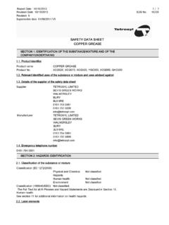
4 Turn On TimeFigure 2. Turn Off TimeSWITCHING TIME EQUIVALENT TEST CIRCUITSS cope rise time < ns*Total shunt capacitance of test jig connectors, and oscilloscope+16 V- V< to 100 ms,DUTY CYCLE kW+ 30 V200 WCS* < 10 pF+16 V-14 V0< 20 to 100 ms,DUTY CYCLE kW+ 30 V200 WCS* < 10 pF- VFigure 3. CapacitancesREVERSE VOLTAGE (VOLTS) 4. Charge DataIC, COLLECTOR CURRENT (mA) (pF)Q, CHARGE (nC) = 30 VIC/IB = 10 CoboQTQA25 C100 CTRANSIENT 5. Turn On TimeIC, COLLECTOR CURRENT (mA) 6. Rise and Fall TimesIC, COLLECTOR CURRENT (mA)t, TIME (ns)t, TIME (ns)701001020507010020030050030IC/IB = 10tr @ VCC = 30 Vtr @ VCC = 10 Vtd @ VEB = Vtd @ VEB = = 30 VIC/IB = 10trtf2N4401 7. Storage TimeIC, COLLECTOR CURRENT (mA)Figure 8. Fall TimeIC, COLLECTOR CURRENT (mA) , STORAGE TIME (ns) tf, FALL TIME (ns)102050701002003005003010020030705030 01020507010020030050030ts = ts - 1/8 tfIB1 = IB2IC/IB = 10 to 20 VCC = 30 VIB1 = IB2IC/IB = 20IC/IB = 9.
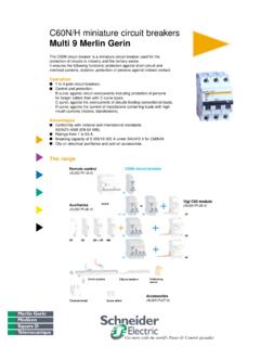
5 Frequency Effectsf, FREQUENCY (kHz)SMALL SIGNAL CHARACTERISTICSNOISE FIGUREVCE = 10 Vdc, TA = 25 C; Bandwidth = HzNF, NOISE FIGURE (dB)IC = mA, RS = 150 WIC = 500 mA, RS = 200 WIC = 100 mA, RS = kWIC = 50 mA, RS = kWRS = OPTIMUMRS = SOURCERS = RESISTANCE100 k50100 200500 k k 10 k20 k50 , NOISE FIGURE (dB)Figure 10. Source Resistance EffectsRS, SOURCE RESISTANCE (OHMS)f = kHzIC = 50 mAIC = 100 mAIC = 500 mAIC = mA2N4401 PARAMETERSVCE = 10 Vdc, f = kHz, TA = 25 CThis group of graphs illustrates the relationship betweenhfe and other h parameters for this series of Transistors . Toobtain these curves, a high gain and a low gain unit wereselected from the 2N4401 lines, and the same units wereused to develop the correspondingly numbered curves oneach 11. Current GainIC, COLLECTOR CURRENT (mA) , CURRENT GAINhie, INPUT IMPEDANCE (OHMS)Figure 12.
6 Input ImpedanceIC, COLLECTOR CURRENT (mA)50 k10 13. Voltage Feedback RatioIC, COLLECTOR CURRENT (mA) 14. Output AdmittanceIC, COLLECTOR CURRENT (mA) , OUTPUT ADMITTANCE ( mhos)oeh , VOLTAGE FEEDBACK RATIO (X 10 )rem-42N4401 UNIT 12N4401 UNIT 22N4401 UNIT 12N4401 UNIT 22N4401 UNIT 12N4401 UNIT 22N4401 UNIT 12N4401 UNIT CHARACTERISTICSF igure 15. DC Current GainIC, COLLECTOR CURRENT (mA)Figure 16. Collector Saturation RegionIB, BASE CURRENT (mA) , COLLECTOR-EMITTER VOLTAGE (VOLTS) = mATJ = 25 mA100 mA102030500 , NORMALIZED CURRENT = 125 C- 55 CVCE = VVCE = 10 VFigure 17. On VoltagesIC, COLLECTOR CURRENT (mA) 18. Temperature CoefficientsIC, COLLECTOR CURRENT (mA)VOLTAGE (VOLTS) + = 25 CVBE(sat) @ IC/IB = 10 VCE(sat) @ IC/IB = 10 VBE @ VCE = 10 VqVC for VCE(sat)qVB for (mV/ C) - DIMENSIONSTO 92 (TO 226)CASE 29 11 ISSUE AMNOTES:1.
7 DIMENSIONING AND TOLERANCING PER , CONTROLLING DIMENSION: CONTOUR OF PACKAGE BEYOND DIMENSION RIS LEAD DIMENSION IS UNCONTROLLED IN P ANDBEYOND DIMENSION K X XCVDNNXXSEATINGPLANEDIM MINMAXMIN :1. DIMENSIONING AND TOLERANCING PERASME , CONTROLLING CONTOUR OF PACKAGE BEYONDDIMENSION R IS LEAD DIMENSION IS UNCONTROLLED INP AND BEYOND DIMENSION K X XCVDNXXSEATINGPLANEDIM LEADBULK PACKBENT LEADTAPE & REELAMMO PACKSTYLE 1:PIN Semiconductor and are registered trademarks of Semiconductor Components Industries, LLC (SCILLC). SCILLC reserves the right to make changes without further noticeto any products herein. SCILLC makes no warranty, representation or guarantee regarding the suitability of its products for any particular Purpose , nor does SCILLC assume anyliability arising out of the application or use of any product or circuit, and specifically disclaims any and all liability, including without limitation special, consequential or incidentaldamages.
8 Typical parameters which may be provided in SCILLC data sheets and/or specifications can and do vary in different applications and actual performance may vary overtime. All operating parameters, including Typicals must be validated for each customer application by customer s technical experts. SCILLC does not convey any license underits patent rights nor the rights of others. SCILLC products are not designed, intended, or authorized for use as components in systems intended for surgical implant into the body,or other applications intended to support or sustain life, or for any other application in which the failure of the SCILLC product could create a situation where personal injury or deathmay occur. Should Buyer purchase or use SCILLC products for any such unintended or unauthorized application, Buyer shall indemnify and hold SCILLC and its officers, employees,subsidiaries, affiliates, and distributors harmless against all claims, costs, damages, and expenses, and reasonable attorney fees arising out of, directly or indirectly, any claim ofpersonal injury or death associated with such unintended or unauthorized use, even if such claim alleges that SCILLC was negligent regarding the design or manufacture of the is an Equal Opportunity/Affirmative Action Employer.
9 This literature is subject to all applicable copyright laws and is not for resale in any ORDERING INFORMATIONN. American Technical Support: 800 282 9855 Toll FreeUSA/CanadaEurope, Middle East and Africa Technical Support:Phone: 421 33 790 2910 Japan Customer Focus CenterPhone: 81 3 5773 38502N4401/DLITERATURE FULFILLMENT:Literature Distribution Center for ON Box 5163, Denver, Colorado 80217 USAP hone: 303 675 2175 or 800 344 3860 Toll Free USA/CanadaFax: 303 675 2176 or 800 344 3867 Toll Free USA/CanadaEmail: Semiconductor Website: Literature: additional information, please contact your locaSales Representativ