Transcription of 30 MHz to 6 GHz RF/IF Gain Block Data Sheet …
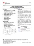
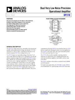
1 30 MHz to 6 GHz RF/IF gain Block data Sheet adl5611 Rev. B Document Feedback Information furnished by analog devices is believed to be accurate and reliable. However, no responsibility is assumed by analog devices for its use, nor for any infringements of patents or other rights of third parties that may result from its use. Specifications subject to change without notice. No license is granted by implication or otherwise under any patent or patent rights of analog devices . Trademarks and registered trademarks are the property of their respective owners. One Technology Way, Box 9106, Norwood, MA 02062-9106, Tel: 2013 2015 analog devices , Inc. All rights reserved. Technical Support FEATURES Fixed gain of dB Broad operation from 30 MHz to 6 GHz High dynamic range gain Block Input and output internally matched to 50 Integrated bias circuit OIP3 of dBm at 900 MHz P1dB of dBm at 900 MHz Noise figure of dB at 900 MHz Single 5 V power supply Low quiescent current of 94 mA Wide operating temperature range of 40 C to +105 C Thermally efficient SOT-89 package ESD rating of kV (Class 1C) FUNCTIONAL Block DIAGRAM Figure 1.
2 GENERAL DESCRIPTION The adl5611 is a single-ended RF/IF gain Block amplifier that provides broadband operation from 30 MHz to 6 GHz. The adl5611 provides a low noise figure of dB with a very high OIP3 of dBm simultaneously, which delivers a high dynamic range. The adl5611 provides a gain of dB that is stable over frequency, temperature, and power supply, and from device to device. The amplifier is offered in the industry-standard SOT-89 package and is internally matched to 50 at the input and output, making the adl5611 easy to implement in a wide variety of applications. The only external parts required are the input and output ac coupling capacitors, power supply decoupling capacitors, and bias inductor. The adl5611 has a high ESD rating of kV (Class 1C) and is fully specified for operation across a wide temperature range of 40 C to +105 C. A fully populated RoHS compliant evaluation board is available.
3 GND12 BIAS3 GNDADL5611(2)RFINRFOUT11508-001 adl5611 data Sheet Rev. B | Page 2 of 16 TABLE OF CONTENTS Features .. 1 Functional Block Diagram .. 1 General Description .. 1 Revision History .. 2 Specifications .. 3 Typical Scattering Parameters (S-Parameters) .. 5 Absolute Maximum Ratings .. 7 Thermal Resistance .. 7 ESD Caution .. 7 Pin Configuration and Function Descriptions .. 8 Typical Performance Characteristics .. 9 500 MHz to 6 GHz Frequency Band .. 9 30 MHz to 500 MHz Frequency Band .. 10 11 Applications Information .. 13 Basic Connections .. 13 Soldering Information and Recommended PCB Land 14 W-CDMA ACPR Performance .. 14 Evaluation Board .. 15 Outline Dimensions .. 16 Ordering Guide .. 16 REVISION HISTORY 12/15 Rev. A to Rev. B Updated Outline Dimensions .. 16 9/13 Rev. 0 to Rev. A Added Figure 19; Renumbered Sequentially .. 11 Changes to Figure 29 .. 14 Updated Outline Dimensions.
4 16 7/13 Revision 0: Initial Version data Sheet adl5611 Rev. B | Page 3 of 16 SPECIFICATIONS VPOS = 5 V and TA = 25 C, unless otherwise noted. Table 1. Parameter Test Conditions/Comments Min Typ Max Unit OVERALL FUNCTION Frequency Range 30 6000 MHz FREQUENCY = 30 MHz gain dB Output 1 dB Compression Point (P1dB) dBm Output Third-Order Intercept (OIP3) f = 1 MHz, output power (POUT) = 0 dBm per tone dBm Noise Figure1 dB FREQUENCY = 140 MHz gain dB vs. Frequency 10 MHz dB vs. Temperature 40 C TA +105 C dB vs. Supply V to V dB Output 1 dB Compression Point dBm Output Third-Order Intercept f = 1 MHz, POUT = 0 dBm per tone dBm Noise Figure1 dB FREQUENCY = 350 MHz gain dB vs. Frequency 10 MHz dB vs. Temperature 40 C TA +105 C dB vs. Supply V to V dB Output 1 dB Compression Point dBm Output Third-Order Intercept f = 1 MHz, POUT = 0 dBm per tone dBm Noise Figure1 dB FREQUENCY = 700 MHz gain dB vs.
5 Frequency 50 MHz dB vs. Temperature 40 C TA +105 C dB vs. Supply V to V dB Output 1 dB Compression Point dBm Output Third-Order Intercept f = 1 MHz, POUT = 0 dBm per tone dBm Noise Figure1 dB FREQUENCY = 900 MHz gain dB vs. Frequency 50 MHz dB vs. Temperature 40 C TA +105 C dB vs. Supply V to V dB Output 1 dB Compression Point dBm Output Third-Order Intercept f = 1 MHz, POUT = 0 dBm per tone dBm Noise Figure1 dB FREQUENCY = 1900 MHz gain dB vs. Frequency 50 MHz dB vs. Temperature 40 C TA +105 C dB vs. Supply V to V dB Output 1 dB Compression Point dBm Output Third-Order Intercept f = 1 MHz, POUT = 0 dBm per tone dBm Noise Figure1 dB adl5611 data Sheet Rev. B | Page 4 of 16 Parameter Test Conditions/Comments Min Typ Max Unit FREQUENCY = 2140 MHz gain dB vs.
6 Frequency 50 MHz dB vs. Temperature 40 C TA +105 C dB vs. Supply V to V dB Output 1 dB Compression Point dBm Output Third-Order Intercept f = 1 MHz, POUT = 0 dBm per tone dBm Noise Figure1 dB FREQUENCY = 2600 MHz gain dB vs. Frequency 50 MHz dB vs. Temperature 40 C TA +105 C dB vs. Supply V to V dB Output 1 dB Compression Point dBm Output Third-Order Intercept f = 1 MHz, POUT = 0 dBm per tone dBm Noise Figure1 dB FREQUENCY = 3500 MHz gain dB vs. Frequency 50 MHz dB vs. Temperature 40 C TA +105 C dB vs. Supply V to V dB Output 1 dB Compression Point dBm Output Third-Order Intercept f = 1 MHz, POUT = 0 dBm per tone dBm Noise Figure1 dB FREQUENCY = 4000 MHz gain dB vs. Frequency 50 MHz dB vs. Temperature 40 C TA +105 C dB vs. Supply V to V dB Output 1 dB Compression Point dBm Output Third-Order Intercept f = 1 MHz, POUT = 0 dBm per tone dBm Noise Figure1 dB FREQUENCY = 5000 MHz gain dB vs.
7 Frequency 50 MHz dB vs. Temperature 40 C TA +105 C dB vs. Supply V to V dB Output 1 dB Compression Point dBm Output Third-Order Intercept f = 1 MHz, POUT = 0 dBm per tone dBm Noise Figure1 dB FREQUENCY = 5800 MHz gain dB vs. Frequency 50 MHz dB vs. Temperature 40 C TA +105 C dB vs. Supply V to V dB Output 1 dB Compression Point dBm Output Third-Order Intercept f = 1 MHz, POUT = 0 dBm per tone dBm Noise Figure1 dB data Sheet adl5611 Rev. B | Page 5 of 16 Parameter Test Conditions/Comments Min Typ Max Unit POWER INTERFACE Supply Voltage VPOS 5 V Supply Current 94 124 mA vs. Temperature 40 C TA +105 C 7/+14 mA Power Dissipation VPOS = 5 V 470 mW 1 Noise figure specified includes printed circuit board (PCB) traces losses. TYPICAL SCATTERING PARAMETERS (S-PARAMETERS) VPOS = 5 V and TA = 25 C.
8 Table 2. Frequency (MHz) S11 S21 S12 S22 Magnitude (dB) Angle ( ) Magnitude (dB) Angle ( ) Magnitude (dB) Angle ( ) Magnitude (dB) Angle ( ) 30 + + + 50 + + + 100 + + 200 + + 300 + + 400 + + 500 + 600 + 700 + 800 + 900 + 1000 + 1100 + 1200 + 1300 + 1400 + 1500 + 1600 + 1700 + 1800 + 1900 + 2000 + 2100 + 2200 + 2300 + 2400 + 2500 + 2600 + 2700 + 2800 + 2900 + 3000 +
9 3100 + 3200 + 3300 + 3400 + 3500 + adl5611 data Sheet Rev. B | Page 6 of 16 Frequency (MHz) S11 S21 S12 S22 Magnitude (dB) Angle ( ) Magnitude (dB) Angle ( ) Magnitude (dB) Angle ( ) Magnitude (dB) Angle ( ) 3600 + 3700 + 3800 + 3900 + 4000 + 4100 + 4200 + 4300 + 4400 + 4500 + 4600 + 4700 + 4800 + 4900 + 5000 + 5100 + 5200 + 5300 + 5400 + 5500 + 5600 + 5700 + 5800 + 5900 + 6000 + data Sheet adl5611 Rev.
10 B | Page 7 of 16 ABSOLUTE MAXIMUM RATINGS Table 3. Parameter Rating Supply Voltage, VPOS V Input Power (50 Impedance) 20 dBm Internal Power Dissipation (Pad Soldered to Ground) 800 mW ESD Human Body Model (HBM) Rating (ESDA/ JEDEC JS-001-2011) kV Maximum Junction Temperature 150 C Operating Temperature Range 40 C to +105 C Storage Temperature Range 65 C to +150 C Stresses at or above those listed under Absolute Maximum Ratings may cause permanent damage to the product. This is a stress rating only; functional operation of the product at these or any other conditions above those indicated in the operational section of this specification is not implied. Operation beyond the maximum operating conditions for extended periods may affect product reliability. THERMAL RESISTANCE Ta b l e 4 lists the junction-to-air thermal resistance ( JA) and the junction-to-case thermal resistance ( JC) for the adl5611 .