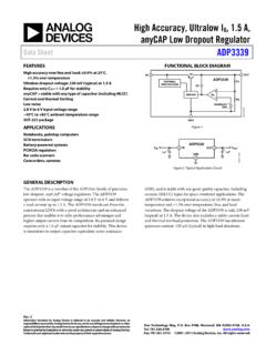
Transcription of 4.5 V to 20 V Input, 15 A, 25 A, 40 A microBuck DC/DC ...
1 SiC450, SiC451, Siliconix S21-0213-Rev. B, 08-Mar-20211 Document Number: 77863 For technical questions, contact: DOCUMENT IS SUBJECT TO CHANGE WITHOUT NOTICE. THE PRODUCTS DESCRIBED HEREIN AND THIS DOCUMENTARE SUBJECT TO SPECIFIC DISCLAIMERS, SET FORTH AT V to 20 V Input, 15 A, 25 A, 40 A microBuck DC/DC Converter With PMBus InterfaceLINKS TO ADDITIONAL RESOURCESDESCRIPTIONThe SiC45x is a PMBus compliant non-isolated DC/DC buck regulator with integrated MOSFETs. It is capable of supplying up to 40 A (SiC450) continuous output current . Its output voltage is digitally adjustable from V to 12 V from a V to 20 V input with switching frequencies up to MHz.
2 SiC45x architecture delivers ultrafast transient response with minimum output capacitance and tight regulation over a broad load range. The device has integrated internal compensation and is stable with any type of output capacitor. The device incorporates a power saving scheme that significantly increases light load SiC45x allows power block configuration programs to be stored in non volatile memory (NVM). Various operation parameters can all be locally stored and used to determine fault behavior. Operation is firmware based and is field upgradable Pinstrap option is also available for default configuration without SiC45x is available in lead (Pb)-free power enhanced MLP 5 mm x 7 mm APPLICATION CIRCUIT Fig.
3 1 - Typical Application CircuitFEATURES Versatile- Single supply operation from V to 20 V input voltage- Scalable solution with continuous output current of 40 A (SiC450), 25 A (SiC451), 15 A (SiC453)- Adjustable output voltage from V to 12 V- Built in 5 V regulator for internal circuits and driver supply- 1 % output voltage accuracy over temperature- Ultrafast transient response Highly efficient- 98 % peak efficiency- Optional power save mode Highly configurable- PMBus compliant with 1 MHz bus speed- Internal NVM- VOUT adjustability and reading resolution of 2 mV- Supports over 50 PMBus commands- Supports in phase or 180 out of phase synchronization- output voltage source and sink capability Robust and reliable- PVIN, VOUT.
4 IIN and IOUT and temperature reporting - Over current protection in pulse-by-pulse mode- output over and under voltage protection - Over temperature protection with hysteresis- Differential output remote sensingAPPLICATIONS Server, cloud, and infrastructure Networking, telecom, storage applications Distributed point of load power architectures DDR memory Fig. 2 - SiC450 Efficiency CurveDesign ToolEvaluationBoardsDesign V to 20 VENVOUTAGNDPGNDSiC45xVSETRT/SYNCADDRVDDP VCCPVINBOOTPGOODENABLEPGOODSWVSEN+SALRTS DASCLVSEN- PH10100100010000808284868890929496980510 152025303540 Axis Title1st line2nd line2nd lineeff - Efficiency (%)IOUT- output current (A) Vo5 VoVIN = 12 VFsw = 600 kHzSiC450, SiC451, Siliconix S21-0213-Rev.
5 B, 08-Mar-20212 Document Number: 77863 For technical questions, contact: DOCUMENT IS SUBJECT TO CHANGE WITHOUT NOTICE. THE PRODUCTS DESCRIBED HEREIN AND THIS DOCUMENTARE SUBJECT TO SPECIFIC DISCLAIMERS, SET FORTH AT CONFIGURATION Fig. 3 - Pin Configuration - Bottom ViewPIN DESCRIPTIONPIN NUMBERSYMBOL DESCRIPTION1, 2, 3, 34 PVINI nput voltage for power stage4 PHPhase node, return path of high side gate driver5 GHHigh side MOSFET gate monitor6 BOOTB ootstrap voltage for high side gate driver (referenced to PH)7, 16 AGNDA nalog signal return ground8 NCNot used in Vishay device9 NCNot used in Vishay device10 NCNot used in Vishay device11 VSEN-Remote sense amplifier negative input connect to output ground12 VSEN+Remote sense amplifier positive input connect to output13 PGOODP ower good.
6 Open-drain output indicating VOUT is within set limits. Connect a pull up resistor typically 10 k to VDD14 ADDRPMBus address programming pin15 VSETO utput voltage set point by connecting a resistor from VSET to AGND17RT/SYNCC lock synchronization pin. Frequency can be set by connecting a resistor to AGND. Pending on master / salve configuration, a clock can be send / receive via the pin18 SALRTPMBus alert. Connect to external host interface if desired19 SDAPMBus data. Connect to external host interface20 SCLPMBus clock. Connect to external host interface21 ENEnable pin. Active high 5 V logic level input22 VDDI nternal 5 V circuits supply voltage.
7 VDD is a LDO output , connect a 1 F decoupling capacitor to AGND23 VINI nternal driver supply voltage24 PVCCS upply voltage for internal gate drive. PVCC is a LDO output . Connect a F decoupling capacitor to PGND25 GLLow side MOSFET gate monitor26 to 31 SWSwitch node32, 33 PGNDP ower ground. Common return for internal MOSFETsORDERING INFORMATIONPART NUMBER PART MARKINGMAXIMUM CURRENTPACKAGE SiC450ED-T1-GE3 SiC45040 APowerPAK MLP34-57 SiC450 EVBR eference boardSiC451ED-T1-GE3 SiC45125 APowerPAK MLP34-57 SiC451 EVBR eference boardSiC453ED-T1-GE3 SiC45315 APowerPAK MLP34-57 SiC453 EVBR eference boardNC 9NC 8 AGND 7 BOOT 6 GH 5PH 4 PVIN 3 PVIN 2 PVIN 1 PGND 33 PVIN 34 SW 3130 SW25 GL24 PVCC23 VIN22 VDD21 EN20 SCL 19 SDA 18 SALRT 17 RT / SYNC 16 AGND15 VSET14 ADDR13 PGOOD12 VSEN+ 11 VSEN-10 NC PGND 3229 SW28 SW27 SW26 SWSiC450, SiC451, Siliconix S21-0213-Rev.
8 B, 08-Mar-20213 Document Number: 77863 For technical questions, contact: DOCUMENT IS SUBJECT TO CHANGE WITHOUT NOTICE. THE PRODUCTS DESCRIBED HEREIN AND THIS DOCUMENTARE SUBJECT TO SPECIFIC DISCLAIMERS, SET FORTH AT MARKING INFORMATION Stresses beyond those listed under Absolute Maximum Ratings may cause permanent damage to the device. These are stress ratings only, and functional operation of the device at these or any other conditions beyond those indicated in the operational sections of the specifications is not implied. Exposure to absolute maximum rating / conditions for extended periods may affect device MAXIMUM RATINGS (TA = 25 C, unless otherwise noted)ELECTRICAL PARAMETER CONDITIONSLIMITSUNIT PVIN, VINR eference to to +28 VSW / PHReference to to +28SW / PH (AC)Reference to PGND (100 ns)-8 to +33 BOOT to VPH + PVCCBOOT to to +6 Drive supply voltage (PVCC) to +6 Bias supply voltage (VDD) to +6 AGND to to + other pinsReference to to VDD + temperature-40 to +150 CStorage temperature-65 to +150 Power DissipationJunction-to-ambient thermal impedance (RthJA)
9 24 C/WThermal resistance from junction to case (RthJ-C) resistance from junction to PCB (RthJ-PCB)5 ESD ProtectionElectrostatic discharge protectionHBM2kVCDM750 VRECOMMENDED OPERATING CONDITIONS (all voltages referenced to GND = 0 V)ELECTRICAL PVIN, supply voltage (PVCC) supply voltage (VDD) ambient temperature-40 to +85 COperating junction temperature-40 to +125=pin 1 indicatorP/N =part number code=Siliconix logo =ESD symbolF=assembly factory codeY=year codeWW =week codeLL=lot codeF Y W WP/NLLSiC450, SiC451, Siliconix S21-0213-Rev. B, 08-Mar-20214 Document Number: 77863 For technical questions, contact: DOCUMENT IS SUBJECT TO CHANGE WITHOUT NOTICE.
10 THE PRODUCTS DESCRIBED HEREIN AND THIS DOCUMENTARE SUBJECT TO SPECIFIC DISCLAIMERS, SET FORTH AT SPECIFICATIONS (PVIN = 12 V, TJ = -40 C to +125 C, unless otherwise specified)PARAMETER SYMBOLTEST CONDITIONSLIMITSUNIT MIN. SuppliesPVIN, VINPVIN, , defaultVIN_ONDefault setting-10-VIN_OFF, defaultVIN_OFFD efault setting-9-PVCC supplyVPVCCVIN = V to 20 supplyVDDL ogic supply UVLO UVLO hysteresisVPVCC_UVLO_HYS-300-mVInput currentIVINTJ = 25 C, non-switching, no load, VOUT > VSET, IPVCC + IPVDD + currentIVIN_SDNEN = 0 V, IPVCC + IPVDD + MonitoringPVIN monitor accuracyVPVIN_MON_ACC-3-%PVIN min.