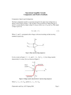
Transcription of 50 µA, 2 mm × 1.7 mm WLCSP, Low Noise, Heart Rate Monitor ...
1 50 A, 2 mm mm WLCSP, Low Noise, Heart Rate Monitor for Wearable ProductsData Sheet AD8233 Rev. 0 Document Feedback Information furnished by Analog Devices is believed to be accurate and reliable. However, no responsibility is assumed by Analog Devices for its use, nor for any infringements of patents or other rights of third parties that may result from its use. Specifications subject to change without notice. No license is granted by implication or otherwise under any patent or patent rights of Analog Devices. Trademarks and registered trademarks are the property of their respective owners.
2 One Technology Way, Box 9106, Norwood, MA 02062-9106, : 2016 Analog Devices, Inc. All rights reserved. Technical Support FEATURES Fully integrated, single-lead electrocardiogram (ECG) front end Low quiescent supply current: 50 A (typical) Leads on/off detection while in shutdown (<1 A) Common-mode rejection ratio: 80 dB (dc to 60 Hz) 2 or 3 electrode configurations High signal gain (G = 100) with dc blocking capabilities 2-pole adjustable high-pass filter Accepts up to 300 mV of half cell potential Fast restore feature improves filter settling Uncommitted op amp 3-pole adjustable low-pass filter with adjustable gain Integrated right leg drive (RLD) amplifier with shutdown Single-supply operation.
3 V to V Integrated reference buffer generates virtual ground Rail-to-rail output Internal RFI filter 8 kV human body model (HBM) ESD rating Shutdown pin 2 mm mm WLCSP APPLICATIONS Fitness and activity Heart rate monitors Portable ECG Wearable and remote health monitors Gaming peripherals Biopotential signal acquisition, such as EMG FUNCTIONAL BLOCK DIAGRAM LODAD8233+VSGNDOPAMP OUTREFOUTOPAMP+SWREFINIAOUTHPSENSEHPDRIV E+IN INRLDRLDFBFRSDNAC/DCLEADS OFFDETECTION10k 10k 150k S1S2A4B5A5C5C4B4A3A2A1B3 IAA3D5D4D3C3D2D1A1A2B2B1C2C1 CRLD SDN13737-001 Figure 1. GENERAL DESCRIPTION The AD8233 is an integrated signal conditioning block for ECG and other biopotential measurement applications.
4 It is designed to extract, amplify, and filter small biopotential signals in the presence of noisy conditions, such as those created by motion or remote electrode placement. This design allows an ultralow power analog-to-digital converter (ADC) or an embedded microcontroller to easily acquire the output signal. The AD8233 implements a two-pole high-pass filter for eliminating motion artifacts and the electrode half cell potential. This filter is tightly coupled with the instrumentation architec-ture of the amplifier to allow both large gain and high-pass filtering in a single stage, thereby saving space and cost.
5 An uncommitted operational amplifier enables the AD8233 to create a three-pole, low-pass filter to remove additional noise. The user can select the frequency cutoff of all filters to suit different types of applications. To improve the common-mode rejection of the line frequencies in the system and other undesired interferences, the AD8233 includes an amplifier for driven lead applications, RLD. The AD8233 includes a fast restore function that reduces the duration of the otherwise long settling tails of the high-pass filters. After an abrupt signal change that rails the amplifier (such as a leads off condition), the AD8233 automatically adjusts to a higher filter cutoff.
6 This feature allows the AD8233 to recover quickly, and therefore, to take valid measurements soon after connecting the electrodes to the subject. The AD8233 is available in a 2 mm mm, 20-ball WLCSP package. Performance is specified from 0 C to 70 C and is operational from 40 C to +85 C. Table 1. AD8232 vs. AD8233 Comparison Parameter AD8232 AD8233 Supply Current 170 A 50 A Peak-to-Peak Voltage Noise (f = Hz to 40 Hz) 14 V p-p V Leads On/Off Detection in Shutdown Not included Included Right Leg Drive Shutdown Not included Included Package Size 4 mm 4 mm mm 2 mm mm mm AD8233* PRODUCT PAGE QUICK LINKSLast Content Update: 02/23/2017 COMPARABLE PARTSView a parametric search of comparable KITS AD8233 Evaluation BoardDOCUMENTATIONData Sheet AD8233.
7 50 A, 2 mm mm WLCSP, Low Noise, Heart Rate Monitor for Wearable Products Data SheetUser Guides UG-1016: Evaluating the AD8233 50 A, 2 mm mm WLCSP, Low Noise, Heart Rate Monitor for Wearable ProductsTOOLS AND SIMULATIONS AD8232/AD8233 Filter Design Tool AD8233 SPICE Macro-ModelREFERENCE MATERIALSP ress Analog Devices Low Power AFE Enables Smaller, Lighter Wearable Health Devices with Longer Battery LifeSolutions Bulletins & Brochures Technologies and Applications for the Internet of ThingsWhite Papers Operating the AD8233 with the ADuCM350 DESIGN RESOURCES AD8233 Material Declaration PCN-PDN Information Quality And Reliability Symbols and FootprintsDISCUSSIONSView all AD8233 EngineerZone AND BUYV isit the product page to see pricing SUPPORTS ubmit a technical question or find your regional support FEEDBACKS ubmit feedback for this data page is dynamically generated by Analog Devices, Inc.
8 , and inserted into this data sheet. A dynamic change to the content on this page will not trigger a change to either the revision number or the content of the product data sheet. This dynamic page may be frequently Data Sheet Rev. 0 | Page 2 of 29 TABLE OF CONTENTS Features .. 1 Applications .. 1 Functional Block Diagram .. 1 General Description .. 1 Revision History .. 2 Specifications .. 3 Absolute Maximum Ratings .. 6 Thermal Resistance .. 6 Pin Configuration and Function Descriptions .. 7 Typical Performance Characteristics .. 8 Instrumentation amplifier Performance Characteristics.
9 8 operational amplifier Performance Characteristics .. 11 Right Leg Drive (RLD) amplifier Performance Characteristics .. 14 Reference Buffer Performance Characteristics .. 15 System Performance Characteristics .. 16 Theory of Operation .. 17 Architecture Overview .. 17 Instrumentation amplifier .. 17 operational amplifier .. 17 Right Leg Drive amplifier .. 18 Reference Buffer .. 18 Fast Restore Circuit .. 18 Leads On/Off Detection .. 19 Standby Operation .. 20 Input Protection .. 21 Radio Frequency Interference (RFI) .. 21 Power Supply Regulation and Bypassing .. 21 Input Referred Offsets.
10 21 Layout Recommendations .. 21 Applications Information .. 22 Eliminating Electrode 22 High-Pass Filtering .. 22 Low-Pass Filtering and Gain .. 24 Driven Electrode .. 25 Application Circuits .. 26 Heart Rate Measurement (HRM) Next to the Heart .. 26 Exercise Application Heart Rate Measured at the Hands .. 26 Holter Monitor Configuration .. 27 Synchronized ECG and PPG Measurement .. 28 Packaging and Ordering Information .. 29 Outline Dimensions .. 29 Ordering Guide .. 29 REVISION HISTORY 8/2016 Revision 0: Initial Version Data Sheet AD8233 Rev. 0 | Page 3 of 29 SPECIFICATIONS +VS = V to 3 V , VREF = +VS/2, VCM = +VS/2, TA = 25 C, FR = low, SDN = high, AC/DC = low, RLD SDN = low, unless otherwise noted.