Transcription of 500mA, Low Noise, LDO Micropower Regulators - …
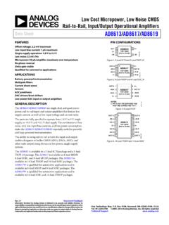
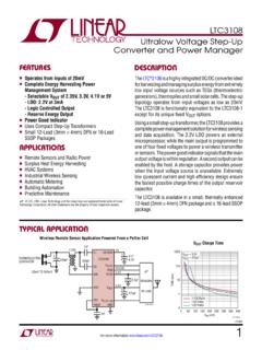
1 For more information Series11763fhTypical applicaTionDescripTion500mA, low noise , LDO Micropower RegulatorsThe LT 1763 series are Micropower , low noise , low dropout Regulators . The devices are capable of supplying 500ma of output current with a dropout voltage of 300mV. Designed for use in battery-powered systems, the low 30 A quiescent current makes them an ideal choice. Quiescent current is well controlled; it does not rise in dropout as it does with many other key feature of the LT1763 Regulators is low output noise . With the addition of an external F bypass capacitor, output noise drops to 20 VRMS over a 10Hz to 100kHz bandwidth. The LT1763 Regulators are stable with output capacitors as low as F. Small ceramic capacitors can be used without the series resistance required by other protection circuitry includes reverse battery protection, current limiting, thermal limiting and reverse current protection.
2 The parts come in fixed output voltages of , , , 3V, and 5V, and as an adjustable device with a reference voltage. The LT1763 regu-lators are available in 8-lead SO and 12-lead, low profile (4mm 3mm ) DFN low noise RegulatorFeaTuresapplicaTionsn low noise : 20 VRMS (10Hz to 100kHz)n Output Current: 500mAn Low Quiescent Current: 30 An Wide Input Voltage Range: to 20Vn Low Dropout Voltage: 300mVn Very Low Shutdown Current: < 1 An No Protection Diodes Neededn Fixed Output Voltages: , , , 3V, , 5Vn Adjustable Output from to 20Vn Stable with F Output Capacitorn Stable with Aluminum, Tantalum or Ceramic Capacitorsn Reverse Battery Protectionn No Reverse Currentn Overcurrent and Overtemperature Protectedn 8-Lead SO and 12-Lead (4mm 3mm) DFN Packagesn Cellular Phonesn Battery-Powered Systemsn noise -Sensitive Instrumentation SystemsDropout F10 F1763 AT 500mA20 VRMS NOISE1 F+OUTPUT CURRENT (mA)0 DROPOUT VOLTAGE (mV)4003503002502001501005004001763 TA02100200300500L, LT, LTC, LTM, Linear Technology and the Linear logo are registered trademarks and ThinSOT is a trademark of Linear Technology Corporation.
3 All other trademarks are the property of their respective owners. Protected by Patents including 6144250, more information Series21763fhabsoluTe MaxiMuM raTingsIN Pin Voltage .. 20 VOUT Pin Voltage .. 20 VInput to Output Differential Voltage .. 20 VSENSE Pin Voltage .. 20 VADJ Pin Voltage .. 7 VBYP Pin Voltage .. Pin Voltage .. 20 VOutput Short-Circuit Duration .. Indefinite(Note 1)12111098713 GND123456 NCININNCSHDNGNDNCOUTOUTNCSENSE/ADJ*BYPTO P VIEWDE PACKAGE12-LEAD (4mm 3mm) PLASTIC DFN TJMAX = 125 C, JA = 40 C/W, JC = 5 C/W EXPOSED PAD (PIN 13) IS GND, MUST BE SOLDERED TO PCB*PIN 5: SENSE FOR FOR LT1763 SEE THE APPLICATIONS INFORMATION VIEWINGNDGNDSHDNOUTSENSE/ADJ*GNDBYPS8 PACKAGE8-LEAD PLASTIC SO12348765 TJMAX = 150 C, JA = 70 C/W, JC = 35 C/W*PIN 2: SENSE FOR FOR LT1763 SEE THE APPLICATIONS INFORMATION inForMaTionLEAD FREE FINISHTAPE AND REELPART MARKING*PACKAGE DESCRIPTIONTEMPERATURE RANGELT1763 CDE#PBFLT1763 CDE#TRPBF176312-Lead (4mm 3mm) Plastic DFN 40 C to 125 CLT1763 IDE#PBFLT1763 IDE#TRPBF176312-Lead (4mm 3mm) Plastic DFN 40 C to 125 CLT1763 MPDE#PBFLT1763 MPDE#TRPBF176312-Lead (4mm 3mm) Plastic DFN 55 C to 125 # #TRPBF7631512-Lead (4mm 3mm) Plastic DFN 40 C to 125 # #TRPBF7631512-Lead (4mm 3mm) Plastic DFN 40 C to 125 # #TRPBF 7631512-Lead (4mm 3mm) Plastic DFN 55 C to 125 # #TRPBF7631812-Lead (4mm 3mm) Plastic DFN 40 C to 125 COperating Junction Temperature Range (Note 2) C, I Grade.
4 40 C to 125 C MP Grade .. 55 C to 125 CStorage Temperature Range S8 Package .. 65 C to 150 C DFN Package .. 65 C to 150 CLead Temperature (Soldering, 10 sec) S8 Package ..300 Cpin conFiguraTionFor more information Series31763fhLEAD FREE FINISHTAPE AND REELPART MARKING*PACKAGE DESCRIPTIONTEMPERATURE # #TRPBF7631812-Lead (4mm 3mm) Plastic DFN 40 C to 125 # #TRPBF 7631812-Lead (4mm 3mm) Plastic DFN 55 C to 125 # #TRPBF7632512-Lead (4mm 3mm) Plastic DFN 40 C to 125 # #TRPBF7632512-Lead (4mm 3mm) Plastic DFN 40 C to 125 # #TRPBF 7632512-Lead (4mm 3mm) Plastic DFN 55 C to 125 CLT1763 CDE-3#PBFLT1763 CDE-3#TRPBF1763312-Lead (4mm 3mm) Plastic DFN 40 C to 125 CLT1763 IDE-3#PBFLT1763 IDE-3#TRPBF1763312-Lead (4mm 3mm) Plastic DFN 40 C to 125 CLT1763 MPDE-3#PBFLT1763 MPDE-3#TRPBF1763312-Lead (4mm 3mm) Plastic DFN 55 C to 125 # #TRPBF7633312-Lead (4mm 3mm) Plastic DFN 40 C to 125 # #TRPBF7633312-Lead (4mm 3mm)
5 Plastic DFN 40 C to 125 # #TRPBF 7633312-Lead (4mm 3mm) Plastic DFN 55 C to 125 CLT1763 CDE-5#PBFLT1763 CDE-5#TRPBF1763512-Lead (4mm 3mm) Plastic DFN 40 C to 125 CLT1763 IDE-5#PBFLT1763 IDE-5#TRPBF1763512-Lead (4mm 3mm) Plastic DFN 40 C to 125 CLT1763 MPDE-5#PBFLT1763 MPDE-5#TRPBF1763512-Lead (4mm 3mm) Plastic DFN 55 C to 125 CLT1763CS8#PBFLT1763CS8#TRPBF17638-Lead Plastic SO 40 C to 125 CLT1763IS8#PBFLT1763IS8#TRPBF17638-Lead Plastic SO 40 C to 125 CLT1763 MPS8#PBFLT1763 MPS8#TRPBF1763MP8-Lead Plastic SO 55 C to 125 # #TRPBF1763158-Lead Plastic SO 40 C to 125 # #TRPBF1763158-Lead Plastic SO 40 C to 125 # #TRPBF1763188-Lead Plastic SO 40 C to 125 # #TRPBF1763188-Lead Plastic SO 40 C to 125 # #TRPBF1763258-Lead Plastic SO 40 C to 125 # #TRPBF1763258-Lead Plastic SO 40 C to 125 # #TRPBF1763258-Lead Plastic SO 55 C to 125 CLT1763CS8-3#PBFLT1763CS8-3#TRPBF176338- Lead Plastic SO 40 C to 125 CLT1763IS8-3#PBFLT1763IS8-3#TRPBF176338- Lead Plastic SO 40 C to 125 # #TRPBF1763338-Lead Plastic SO 40 C to 125 # #TRPBF1763338-Lead Plastic SO 40 C to 125 CLT1763CS8-5#PBFLT1763CS8-5#TRPBF176358- Lead Plastic SO
6 40 C to 125 CLT1763IS8-5#PBFLT1763IS8-5#TRPBF176358- Lead Plastic SO 40 C to 125 CLT1763 MPS8-5#PBFLT1763 MPS8-5#TRPBF176358-Lead Plastic SO 55 C to 125 CConsult LTC Marketing for parts specified with wider operating temperature ranges. *The temperature grade is identified by a label on the shipping container. Consult LTC Marketing for information on nonstandard lead based finish more information on lead free part marking, go to: For more information on tape and reel specifications, go to: inForMaTionFor more information Series41763fhelecTrical characTerisTicsPARAMETERCONDITIONSMINTYP MAXUNITSM inimum Operating VoltageC, I Grade: ILOAD = 500ma (Notes 3, 11) MP Grade: ILOAD = 500ma (Notes 3, 11)l VRegulated Output Voltage (Note 4) VIN = 2V, ILOAD = 1mA < VIN < 20V, 1mA < ILOAD < 500ma VIN = , ILOAD = 1mA < VIN < 20V, 1mA < ILOAD < 500ma VIN = 3V, ILOAD = 1mA < VIN < 20V, 1mA < ILOAD < 500ma VLT1763-3 VIN = , ILOAD = 1mA 4V < VIN < 20V, 1mA < ILOAD < 500ma VIN = , ILOAD = 1mA < VIN < 20V, 1mA < ILOAD < 500ma VLT1763-5 VIN = , ILOAD = 1mA 6V < VIN < 20V, 1mA < ILOAD < 500ma VADJ Pin Voltage (Notes 3, 4)LT1763 VIN = , ILOAD = 1mA C, I Grade: < VIN < 20V, 1mA < ILOAD < 500ma MP Grade: < VIN < 20V, 1mA < ILOAD < 500ma l V VLine C, I Grade: VIN = 2V to 20V, ILOAD = 1mA MP Grade.
7 VIN = to 20V, ILOAD = 1mA VIN = to 20V, ILOAD = 1mA VIN = 3V to 20V, ILOAD = 1mA LT1763-3 VIN = to 20V, ILOAD = 1mA VIN = to 20V, ILOAD = 1mA LT1763-5 VIN = to 20V, ILOAD = 1mA LT1763 (Note 3) C, I Grade: VIN = 2V to 20V, ILOAD = 1mA LT1763 (Note 3) MP Grade: VIN = to 20V, ILOAD = 1mAl l l l l l l l l1 1 1 1 1 1 1 1 15 5 5 5 5 5 5 5 5mV mV mV mV mV mV mV mV mVLoad VIN = , ILOAD = 1mA to 500ma VIN = , ILOAD = 1mA to 500ma l38 15mV VIN = , ILOAD = 1mA to 500ma VIN = , ILOAD = 1mA to 500ma l49 18mV VIN = , ILOAD = 1mA to 500ma VIN = , ILOAD = 1mA to 500ma l512 25mV mVLT1763-3 VIN = 4V, ILOAD = 1mA to 500ma VIN = 4V, ILOAD = 1mA to 500ma l715 30mV VIN = , ILOAD = 1mA to 500ma VIN = , ILOAD = 1mA to 500ma l717 33mV mVLT1763-5 VIN = 6V, ILOAD= 1mA to 500ma VIN = 6V.
8 ILOAD = 1mA to 500ma l1225 50mV mVLT1763 (Note 3) VIN = , ILOAD = 1mA to 500ma C, I Grade: VIN = , ILOAD = 1mA to 500ma MP Grade: VIN = , ILOAD = 1mA to 500ma l l26 12 12mV mV mVDropout Voltage VIN = VOUT(NOMINAL) (Notes 5, 6, 11)ILOAD = 10mA ILOAD = 10mA VILOAD = 50mA ILOAD = 50mA VILOAD = 100mA ILOAD = 100mA VILOAD = 500ma ILOAD = 500ma V The l denotes the specifications which apply over the full operating temperature range, otherwise specifications are at TA = 25 C. (Note 2)For more information Series51763fhelecTrical characTerisTics The l denotes the specifications which apply over the full operating temperature range, otherwise specifications are at TA = 25 C.
9 (Note 2)PARAMETERCONDITIONSMINTYPMAXUNITSGND Pin Current VIN = VOUT(NOMINAL) (Notes 5, 7)ILOAD = 0mA ILOAD = 1mA ILOAD = 50mA ILOAD = 100mA ILOAD = 250mA ILOAD = 500mAl l l l l l30 65 2 5 1175 120 3 8 16 A A mA mA mA mAOutput Voltage NoiseCOUT = 10 F, CBYP = F, ILOAD = 500ma , BW = 10Hz to 100kHz20 VRMSADJ Pin Bias Current(Notes 3, 8)30100nAShutdown ThresholdVOUT = Off to On VOUT = On to Offl l VSHDN Pin Current (Note 9)VSHDN = 0V VSHDN = 1 A AQuiescent Current in ShutdownVIN = 6V, VSHDN = ARipple RejectionVIN VOUT = (Avg), VRIPPLE = , fRIPPLE = 120Hz, ILOAD = 500mA5065dBCurrent LimitVIN = 7V, VOUT = 0V C, I Grade: VIN = VOUT(NOMINAL) + 1V or (Note 12), VOUT = MP Grade: VIN = (Note 12), VOUT = l l 520 520 mA mAInput Reverse Leakage CurrentVIN = 20V, VOUT = 0Vl1mAReverse Output Current (Note 10) VOUT = , VIN < VOUT = , VIN < VOUT = , VIN < LT1763-3 VOUT = 3V, VIN < 3V VOUT = , VIN < LT1763-5 VOUT = 5V, VIN < 5V LT1763 (Note 3) VOUT = , VIN < 10 10 10 10 10 520 20 20 20 20 20 10 A A A A A A ANote 1: Stresses beyond those listed under Absolute Maximum Ratings may cause permanent damage to the device.
10 Exposure to any Absolute Maximum Rating condition for extended periods may affect device reliability and 2: The LT1763 Regulators are tested and specified under pulse load conditions such that TJ @ TA. The LT1763 (C grade) is 100% tested at TA = 25 C; performance at 40 C and 125 C is assured by design, characterization and correlation with statistical process controls. The LT1763 (I grade) is guaranteed over the full 40 C to 125 C operating junction temperature range. The LT1763 (MP grade) is 100% tested and guaranteed over the 55 C to 125 C operating junction temperature 3: The LT1763 (adjustable version) is tested and specified for these conditions with the ADJ pin connected to the OUT 4: Operating conditions are limited by maximum junction temperature. The regulated output voltage specification will not apply for all possible combinations of input voltage and output current.
