Transcription of 8-bit Atmel Microcontroller with 4/8/16K - Farnell …
1 Features High performance, low power Atmel AVR 8-bit Microcontroller Advanced RISC architecture 131 powerful instructions most single clock cycle execution 32 8 general purpose working registers Fully static operation Up to 20 MIPS throughput at 20 MHz On-chip 2-cycle multiplier High endurance non-volatile memory segments 4/8/16 Kbytes of in-system self-programmable flash program memory 256/512/512 bytes EEPROM 512/1K/1 Kbytes internal SRAM Write/erase cyles: 10,000 flash/100,000 EEPROM Data retention.
2 20 years at 85 C/100 years at 25 C(1) Optional boot code section with independent lock bitsIn-system programming by on-chip boot programTrue read-while-write operation Programming lock for software security QTouch library support Capacitive touch buttons, sliders and wheels QTouch and QMatrix acquisition Up to 64 sense channels Peripheral features Two 8-bit timer/counters with separate prescaler and compare mode One 16-bit timer/counter with separate prescaler, compare mode, and capture mode Real time counter with separate oscillator Six PWM channels 8-channel 10-bit ADC in TQFP and QFN/MLF package 6-channel 10-bit ADC in PDIP Package Programmable serial USART Master/slave SPI serial interface Byte-oriented 2-wire serial interface (Philips I2C compatible)
3 Programmable watchdog timer with separate on-chip oscillator On-chip analog comparator Interrupt and wake-up on pin change Special Microcontroller features DebugWIRE on-chip debug system Power-on reset and programmable brown-out detection Internal calibrated oscillator External and internal interrupt sources Five sleep modes: Idle, ADC noise reduction, power-save, power-down, and standby I/O and packages 23 programmable I/O lines 28-pin PDIP, 32-lead TQFP, 28-pad QFN/MLF and 32-pad QFN/MLF Operating voltage: - for Atmel ATmega48V/88V/168V - for Atmel ATmega48/88/168 Temperature range: -40 C to 85 C Speed grade: ATmega48V/88V/168V: 0 - 4 MHz @ - , 0 - 10 MHz @ - ATmega48/88/168: 0 - 10 MHz @ - , 0 - 20 MHz @ - Low power consumption Active mode.
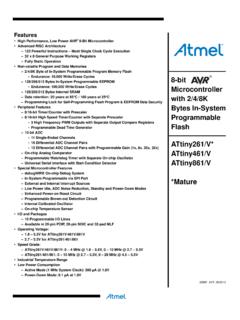
4 250 A at 1 MHz, 15 A at 32kHz, (including oscillator) Power-down mode: A at :1. See Data retention on page 8 for Atmel Microcontroller with 4/8/16K Bytes In-SystemProgrammable FlashATmega48/VATmega88/V ATmega168/V SummaryRev. 2545US AVR 11/201522545US AVR 11/2015 ATmega48/88 configurationsFigure Atmel ATmega48/88 (PCINT19/OC2B/INT1) PD3(PCINT20/XCK/T0) PD4 GNDVCCGNDVCC(PCINT6/XTAL1/TOSC1) PB6(PCINT7/XTAL2/TOSC2) PB7PC1 (ADC1/PCINT9)PC0 (ADC0/PCINT8)ADC7 GNDAREFADC6 AVCCPB5 (SCK/PCINT5)3231302928272625910111213141 516(PCINT21/OC0B/T1) PD5(PCINT22/OC0A/AIN0) PD6(PCINT23/AIN1) PD7(PCINT0/CLKO/ICP1) PB0(PCINT1/OC1A) PB1(PCINT2/SS/OC1B) PB2(PCINT3/OC2A/MOSI) PB3(PCINT4/MISO) PB4PD2 (INT0/PCINT18)PD1 (TXD/PCINT17)PD0 (RXD/PCINT16)
5 PC6 (RESET/PCINT14)PC5 (ADC5/SCL/PCINT13)PC4 (ADC4/SDA/PCINT12)PC3 (ADC3/PCINT11)PC2 (ADC2/PCINT10)TQFP Top View123456789101112131428272625242322212 01918171615(PCINT14/RESET) PC6(PCINT16/RXD) PD0(PCINT17/TXD) PD1(PCINT18/INT0) PD2(PCINT19/OC2B/INT1) PD3(PCINT20/XCK/T0) PD4 VCCGND(PCINT6/XTAL1/TOSC1) PB6(PCINT7/XTAL2/TOSC2) PB7(PCINT21/OC0B/T1) PD5(PCINT22/OC0A/AIN0) PD6(PCINT23/AIN1) PD7(PCINT0/CLKO/ICP1) PB0PC5 (ADC5/SCL/PCINT13)PC4 (ADC4/SDA/PCINT12)PC3 (ADC3/PCINT11)PC2 (ADC2/PCINT10)PC1 (ADC1/PCINT9)PC0 (ADC0/PCINT8)GNDAREFAVCCPB5 (SCK/PCINT5)PB4 (MISO/PCINT4)PB3 (MOSI/OC2A/PCINT3)PB2 (SS/OC1B/PCINT2)PB1 (OC1A/PCINT1)PDIP12345678242322212019181 7323130292827262591011121314151632 MLF Top View(PCINT19/OC2B/INT1) PD3(PCINT20/XCK/T0) PD4 GNDVCCGNDVCC(PCINT6/XTAL1/TOSC1) PB6(PCINT7/XTAL2/TOSC2) PB7PC1 (ADC1/PCINT9)PC0 (ADC0/PCINT8)ADC7 GNDAREFADC6 AVCCPB5 (SCK/PCINT5)(PCINT21/OC0B/T1) PD5(PCINT22/OC0A/AIN0) PD6(PCINT23/AIN1) PD7(PCINT0/CLKO/ICP1) PB0(PCINT1/OC1A) PB1(PCINT2/SS/OC1B) PB2(PCINT3/OC2A/MOSI) PB3(PCINT4/MISO)
6 PB4PD2 (INT0/PCINT18)PD1 (TXD/PCINT17)PD0 (RXD/PCINT16)PC6 (RESET/PCINT14)PC5 (ADC5/SCL/PCINT13)PC4 (ADC4/SDA/PCINT12)PC3 (ADC3/PCINT11)PC2 (ADC2/PCINT10)NOTE: Bottom pad should be soldered to MLF Top View(PCINT19/OC2B/INT1) PD3(PCINT20/XCK/T0) PD4 VCCGND(PCINT6/XTAL1/TOSC1) PB6(PCINT7/XTAL2/TOSC2) PB7(PCINT21/OC0B/T1) PD5(PCINT22/OC0A/AIN0) PD6(PCINT23/AIN1) PD7(PCINT0/CLKO/ICP1) PB0(PCINT1/OC1A) PB1(PCINT2/SS/OC1B) PB2(PCINT3/OC2A/MOSI) PB3(PCINT4/MISO) PB4PD2 (INT0/PCINT18)PD1 (TXD/PCINT17)PD0 (RXD/PCINT16)PC6 (RESET/PCINT14)PC5 (ADC5/SCL/PCINT13)PC4 (ADC4/SDA/PCINT12)PC3 (ADC3/PCINT11)PC2 (ADC2/PCINT10)PC1 (ADC1/PCINT9)PC0 (ADC0/PCINT8)GNDAREFAVCCPB5 (SCK/PCINT5)NOTE.
7 Bottom pad should be soldered to AVR 11/2015 ATmega48/88 supply B (PB7:0) XTAL1/XTAL2/TOSC1/TOSC2 Port B is an 8-bit bi-directional I/O port with internal pull-up resistors (selected for each bit). The Port B output buffers have symmetrical drive characteristics with both high sink and source capability. As inputs, Port B pins that are externally pulled low will source current if the pull-up resistors are activated. The Port B pins are tri-stated when a reset condition becomes active, even if the clock is not on the clock selection fuse settings, PB6 can be used as input to the inverting Oscillator amplifier and input to the internal clock operating on the clock selection fuse settings, PB7 can be used as output from the inverting Oscillator the Internal Calibrated RC Oscillator is used as chip clock source.
8 Is used as input for the Asynchronous Timer/Counter2 if the AS2 bit in ASSR is various special features of Port B are elaborated in Alternate functions of port B on page 83 and System clock and clock options on page C (PC5:0)Port C is a 7-bit bi-directional I/O port with internal pull-up resistors (selected for each bit). The output buffers have symmetrical drive characteristics with both high sink and source capability. As inputs, Port C pins that are externally pulled low will source current if the pull-up resistors are activated.
9 The Port C pins are tri-stated when a reset condition becomes active, even if the clock is not the RSTDISBL Fuse is programmed, PC6 is used as an I/O pin. Note that the electrical characteristics of PC6 differ from those of the other pins of Port the RSTDISBL Fuse is unprogrammed, PC6 is used as a Reset input. A low level on this pin for longer than the minimum pulse length will generate a Reset, even if the clock is not running. The minimum pulse length is given in Table 29-3 on page 314. Shorter pulses are not guaranteed to generate a various special features of Port C are elaborated in Alternate functions of port C on page D (PD7:0)Port D is an 8-bit bi-directional I/O port with internal pull-up resistors (selected for each bit).
10 The Port D output buffers have symmetrical drive characteristics with both high sink and source capability. As inputs, Port D pins that are externally pulled low will source current if the pull-up 42545US AVR 11/2015 ATmega48/88/168resistors are activated. The Port D pins are tri-stated when a reset condition becomes active, even if the clock is not various special features of Port D are elaborated in Alternate functions of port D on page is the supply voltage pin for the A/D Converter, PC3:0, and ADC7:6. It should be externally connected to VCC, even if the ADC is not used.