Transcription of a Frequency-to-Voltage Converter Voltage-to …
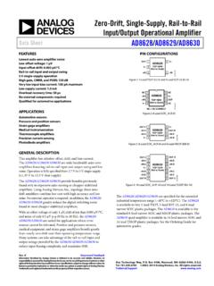
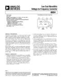
1 REV. BInformation furnished by Analog Devices is believed to be accurate andreliable. However, no responsibility is assumed by Analog Devices for itsuse, nor for any infringements of patents or other rights of third partieswhich may result from its use. No license is granted by implication orotherwise under any patent or patent rights of Analog Technology Way, Box 9106, Norwood, MA 02062-9106, : 781/329-4700 World Wide Web Site: : 781/326-8703 Analog Devices, Inc., 2000 Voltage-to - frequency andFrequency-to- voltage ConverterFEATURESHigh Linearity Max at 10 kHz FS Max at 100 kHz FS Max at 500 kHz FSOutput TTL/CMOS-CompatibleV/F or F/V Conversion6 Decade Dynamic RangeVoltage or Current InputReliable Monolithic ConstructionMIL-STD-883-Compliant Versions AvailablePIN CONFIGURATION(TOP VIEW)N-14 PackageH-10A PackagePRODUCT DESCRIPTIONThe industry standard ADVFC32 is a low cost monolithicvoltage-to- frequency (V/F) Converter or Frequency-to-Voltage (F/V) Converter with good linearity ( max error at 10 kHz)and operating frequency up to MHz.
2 In the V/F configuration,positive or negative input voltages or currents can be convertedto a proportional frequency using only a few external compo-nents. For F/V conversion, the same components are used witha simple biasing network to accommodate a wide range of inputlogic or CMOS compatibility is achieved in the V/F operatingmode using an open collector frequency output. The pull-upresistor can be connected to voltages up to 30 volts, or to 15 Vor 5 V for conventional CMOS or TTL logic levels. This resis-tor should be chosen to limit current through the open collectoroutput to 8 mA. A larger resistance can be used if driving a highimpedance offset drift is only 3 ppm of full scale per C, and full-scale calibration drift is held to a maximum of 100 ppm/ C(ADVFC32BH) due to a low Zener ADVFC32 is available in commercial, industrial, andextended temperature grades.
3 The commercial grade is pack-aged in a 14-lead plastic DIP while the two wider temperaturerange parts are packaged in hermetically sealed 10-lead HIGHLIGHTS1. The ADVFC32 uses a charge balancing circuit technique(see Functional Block Diagram) which is well suited to highaccuracy Voltage-to - frequency conversion. The full-scaleoperating frequency is determined by only one precisionresistor and capacitor. The tolerance of other support compo-nents (including the integration capacitor) is not 20% resistors and capacitors can be used with-out affecting linearity or temperature The ADVFC32 is easily configured to satisfy a wide range ofsystem requirements.
4 Input voltage scaling is set by selectingthe input resistor which sets the input current to mA atthe maximum input The same components used for V/F conversion can also beused for F/V conversion by adding a simple logic biasingnetwork and reconfiguring the The ADVFC32 is intended as a pin-for-pin replacement forVFC32 devices from other The ADVFC32 is available in versions compliant with MIL-STD-883. Refer to the Analog Devices Military ProductsDatabook or current ADVFC32/883B data sheet for B 2 ADVFC32 SPECIFICATIONS(typical @ 25 C with VS = 15 V unless otherwise noted.)ADVFC32 KADVFC32 BADVFC32 SModelMinTypMaxMinTypMaxMinTypMaxUnitDYN AMIC PERFORMANCEFull-Scale frequency Range050005000500kHzNonlinearity1fMAX = 10 kHz + + = 100 kHz + + + = MHz + + + Calibration Error(Adjustable to Zero) 5 5 5%vs.
5 Supply(Full-Scale frequency = 100 kHz) + + + of FSR%vs. Temperature(Full-Scale frequency = 10 kHz) 75 100+100+150+150ppm/ CDYNAMIC RESPONSEM aximum Settling Time for Full ScaleStep Input1 Pulse of New frequency Plus 1 s1 Pulse of New frequency Plus 1 s1 Pulse of New frequency Plus 1 sOverload Recovery Time1 Pulse of New frequency Plus 1 s1 Pulse of New frequency Plus 1 s1 Pulse of New frequency Plus 1 sANALOG INPUT AMPLIFIER(V/F Conversion)Current Input Input Range0 100 100 RIN3 RIN3 RIN3 Differential Impedance300 k ||10 pF2 M ||10 pF300 k ||10 pF 2 M ||10 pF300 k ||10 pF 2 M ||10 pFCommon-Mode Impedance300 M ||3 pF750 M ||3 pF300 M ||3 pF 750 M ||10 pF300 M ||3 pF 750 M ||10 pFInput Bias CurrentNoninverting Input402504025040250nAInverting Input 100 8+100 100 8+100 100 8+100nAInput Offset voltage (Trimmable to Zero)2, 3444mVvs.
6 Temperature (TMIN to TMAX)303030 V/ CSafe Input voltage VS VS VSCOMPARATOR (F/V Conversion)Logic 0 Level VS VS VS 1 Level1+VS1+VS1+VSVP ulse Width sInput Impedance50 k ||10 pF250 k 50 k ||10 pF250 k 50 k ||10 pF250 k OPEN COLLECTOR OUTPUT(V/F Conversion)Output voltage in Logic 0 ISINK = 8 Leakage Current in Logic 1 111 AVoltage Range030030030 VFall Times (Load = 500 pF andISINK = 5 mA)400400400nsAMPLIFIER OUTPUT (F/V Conversion) voltage Range (0 mA IO 7 mA)010010010 VSource Current (0 VO 7 V)101010mACapacitive Load (Without Oscillation)100100100pFClosed Loop Output Impedance111 POWER SUPPLYR ated voltage 15 15 15 VVoltage Range 9 18 9 18 9 18 VQuiescent Current686868mATEMPERATURE RANGES pecified Range0+70 25+85 55+125 COperating Range 25+85 55+125 55+125 CStorage 25+85 65+150 65+150 CPACKAGE OPTIONSP lastic DIP (N-14)ADVFC32 KNTO 100 (H-10A)ADVFC32 BHADVFC32 SHNOTES1 Nonlinearity defined as deviation from a straight line from zero to full scale, expressed as a percentage of full Figure Figure expressed in units of shown in boldface are tested on all production units at final electrical test.
7 Results from those tests are used to calculate outgoing quality levels. All min and max specifications areguaranteed, although only those shown in boldface are tested on all production subject to change without B 3 ADVFC32 UNIPOLAR V/F, POSITIVE INPUT VOLTAGEWhen operated as a V/F Converter , the transformation fromvoltage to frequency is based on a comparison of input signalmagnitude to the 1 mA internal current more complete understanding of the ADVFC32 requires aclose examination of the internal circuitry of this part. Considerthe operation of the ADVFC32 when connected as shown inFigure 1.
8 At the start of a cycle, a current proportional to theFigure 1. Connection Diagram for V/F Conversion,Positive Input Voltageinput voltage flows through R3 and R1 to charge integrationcapacitor C2. As charge builds up on C2, the output voltage ofthe input amplifier decreases. When the amplifier output volt-age (Pin 13) crosses ground (see Figure 2 at time t1), thecomparator triggers a one shot whose time period is determinedby capacitor C1. Specifically, the one shot time period (in nano-seconds) is:tOS (Cl + 44 pF) k Figure 2. Voltage-to - frequency Conversion WaveformsDuring this period, a current of (1 mA IIN) flows out of theintegration capacitor.
9 The total amount of charge depletedduring one cycle is, therefore (1 mA IIN) tOS. This charge isreplaced during the remainder of the cycle to return the integra-tor to its original voltage . Since the charge taken out of C2 isequal to the charge that is put on C2 every cycle,(1 mA IIN) tOS = IIN 1 FOUT tOS or, rearranging terms,FOUT = IIN1mA tOSThe complete transfer equation can now be derived by substi-tuting IIN = VIN/RIN and the equation relating C1 and tOS. Thefinal equation describing ADVFC32 operation is: VIIN/RIN1mA C1+44pF() Components should be selected to optimize performance overthe desired input voltage and output frequency range using theequations listed below: 107pF/secFOUT FS 44pFC2 = 10 4 Farads/secFOUT FS1000pF minimum()RIN = VIN +VLOGIC8mABoth RIN and C1 should have very low temperature coefficientsas changes in their values will result in a proportionate changein the V/F transfer function.
10 Other component values and tem-perature coefficients are not I. Suggested Values for C1, RIN and C2 VIN FSFOUT FSC1 RINC21 V10 kHz3650 k F10 V10 kHz3650 pF40 k F1 V100 kHz330 k 1000 pF10 V100 kHz330 pF40 k 1000 pFORDERING GUIDEPartGain TempcoTemp RangePackageNumber1ppm/ C COptionADVFC32KN 75 typ0 to 7014-PinPlastic DIPADVFC32BH 100 max 25 to +85TO-100 ADVFC32SH 150 max 55 to +125TO-100 NOTE1 For details on grade and package offerings screened in accordance with MIL-STD-883,refer to the Analog Devices Military Products Databook or current ADVFC32/883 Bdata (electrostatic discharge) sensitive device.
