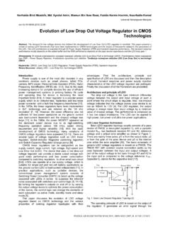
Transcription of A Low-Noise High Power Supply Rejection Low Dropout ...
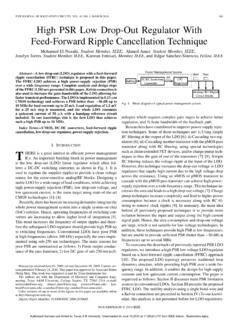
1 A Low-Noise high Power Supply Rejection Low Dropout Regulator for wireless system -on-Chip Applications SIEW KUOK HOON. wireless Analog Technology Center Texas Instruments Inc. Dallas, Texas Outline of Presentation Motivation Conventional Low Dropout Regulator (LDO). Power Supply Rejection Improvement Noise Analysis Experimental Results Conclusion Motivation high Performance LDO : high Power Supply Rejection Low Noise Good Transient Performance. Example of application : RF LDOs in wireless cellular phone. In wireless system -on-Chip(SoC), multiple RF LDOs co-exist. Conventional Low Dropout Regulator (LDO). VDD (Battery Supply , ). VBG (Voltage Reference). ( ). + Pass Element A1. (PMOSFET). - VOUT (Output, ). R1. ILOAD. Resistor feedback (Load Current, network R2 0 to 100mA). CL (Output Capacitor, 1uF). & assoc. ESR res ( Ohms). R1 1 A p1 . VOUT = VBG 1 + . = +. 1.
2 1. R2 . vout vdd A1 g mp rdsp A1 . Power Supply Rejection Improvement vdd Vbg +. ( Power noise +. - assume zero) A1 vout - Subtractor R1. R2. 1 g mN 1 1. Output due to Power noise : v out =. g mp rdsp g mN 2 A1. Power Supply Rejection Boost Circuit MP11. V1. V2. MN1. VDD (Battery Supply ). Cc2 MN1 Pass Element Y (PMOS). Voltage Reference X. V1 Output MN2. V2. CL. Load Current Cc1. Noise Analysis of LDO. Vn2_in - Vn2_O. +. Vn2_BG. R1 Vn2_R1. Vn2_R2. R2. f2 2. R1 2 1 . 2. 1 . 2.. Integrated Noise : Vn _ O 2 . = Vn _ R1 + . 2. Vn _ R1 + Vn _ in + Vn _ BG df . f 1 R2 . Proposed LDO with Dual Output Power f2 1 . 2. Driver 1. = Vn _ in + Vn _ pre df 2 2. Vn _ o . +. f 1 sRC + 1 - Reference Output Voltage (V1). +. Vpre Filter - R2. R1 +. - Output (V2). Power Pre-regulator Driver 2. deep- submicron process : high density (thin oxide) capacitor is available. high sheet rho resistor with min width Chip Micrograph Pre-Regulator Error Amp1.
3 Pre-regulator Error Amp2. Error-Amp PMOS1. Power PMOS. PMOS2. single output Dual-output 2. Noise Measurement of LDO. (with Dual Output Implementation). Integrated noise = (100Hz to 500kHz). Noise Measurement (single output implementation). Integrated noise = (1kHz to 100kHz). ** implemented with smaller area Power Supply Rejection of Proposed and Present Best TOP Proposed BOT Competitor BOT Present Best Proposed 70dB. MP2 MP3 60dB. PSR (dB). 50dB. 40dB. Present Best C1 30dB. MP1. C2. Transient Response Load : 0 to 100mA in 1us 40mV dip 53mV dip Proposed Present Best Conclusion Improvement in both Noise and Power Supply Rejection through : reduction of closed-loop gain 1/ . Advantage is more apparent when Vbg is small ( ), Vout is high ( ). Low Power design possible when resistor divider network can be large (R1, R2). PSR further improved by a subtractor at the Power driver stage.
4 In SoC applications with multiple similar RF LDOs are needed, significant area savings. Current Consumption < 80 A. Noise = 28uVrms (BW= 100Hz to 500kHz). PSR is 60dB at 10kHz