Transcription of AD215 120 kHz Bandwidth, Low Distortion, …
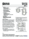
1 A 120 kHz Bandwidth, Low Distortion, Isolation Amplifier AD215 . FEATURES FUNCTIONAL BLOCK DIAGRAM. Isolation Voltage Rating: 1,500 V rms Wide Bandwidth: 120 kHz, Full Power ( 3 dB) FB 4. AD215 . Rapid Slew Rate: 6 V/ms UNCOMMITTED. INPUT OP AMP. Fast Settling Time: 9 ms IN 3. SIGNAL. R R. 38 OUT HI. Low Harmonic Distortion: 80 dB @ 1 kHz IN+ 1. MODULATOR DEMODULATOR. LOW-PASS. FILTER. Low Nonlinearity: IN COM 2. 150kHz T1 OUTPUT. Wide Output Range: 610 V, min (Buffered) BUFFER. 36 TRIM. Built-in Isolated Power Supply: 615 V dc @ 610 mA 33k F. Performance Rated over 408C to +858C 37 OUT LO.
2 POWER. 42 +15 VIN. APPLICATIONS INCLUDE +VISO 6. ISOLATED 430kHz DC POWER 44 15 VIN. High Speed Data Acquisition Systems VISO 5 SUPPLY OSCILLATOR. 43 PWR RTN. T2. Power Line and Transient Monitors Multichannel Muxed Input Isolation Waveform Recording Instrumentation Power Supply Controls Vibration Analysis GENERAL DESCRIPTION Flexible Input and Buffered Output Stages: An uncommit- The AD215 is a high speed input isolation amplifier designed to ted op amp is provided on the input stage of the AD215 to isolate and amplify wide bandwidth analog signals. The innova- allow for input buffering or amplification and signal condition- tive circuit and transformer design of the AD215 ensures wide- ing.
3 The AD215 also features a buffered output stage to drive band dynamic characteristics while preserving key dc performance low impedance loads and an output voltage trim for zeroing the specifications. output offset where needed. The AD215 provides complete galvanic isolation between the High Accuracy: The AD215 has a typical nonlinearity of input and output of the device including the user-available (B grade) of full-scale range and the total harmonic front-end isolated power supplies. The functionally complete distortion is typically 80 dB at 1 kHz. The AD215 provides design, powered by a 15 V dc supply, eliminates the need for a designers with complete isolation of the desired signal without user supplied isolated dc/dc converter.
4 This permits the designer loss of signal integrity or quality. to minimize circuit overhead and reduce overall system design Excellent Common-Mode Performance: The AD215BY. complexity and component costs. (AD215AY) provides 1,500 V rms (750 V rms) common-mode The design of the AD215 emphasizes maximum flexibility and voltage protection from its input to output. Both grades feature ease of use in a broad range of applications where fast analog a low common-mode capacitance of pF inclusive of the signals must be measured under high common-mode voltage dc/dc power isolation.
5 This results in a typical common-mode (CMV) conditions. The AD215 has a 10 V input/output rejection specification of 105 dB and a low leakage current of range, a specified gain range of 1 V/V to 10 V/V, a buffered out- A rms max (240 V rms, 60 Hz). put with offset trim and a user-available isolated front-end Isolated Power: An unregulated isolated power supply of power supply which produces 15 V dc at 10 mA. 15 V dc @ 10 mA is available at the isolated input port of the AD215 . This permits the use of ancillary isolated front-end PRODUCT HIGHLIGHTS amplifiers or signal conditioning components without the need High Speed Dynamic Characteristics: The AD215 features for a separate dc/dc supply.
6 Even the excitation of transducers a typical full-power bandwidth of 120 kHz (100 kHz min), rise can be accomplished in most applications. time of 3 s and settling time of 9 s. The high speed perfor- mance of the AD215 allows for unsurpassed galvanic isolation Rated Performance over the 408C to +858C Temperature of virtually any wideband dynamic signal. Range: With an extended industrial temperature range rating, the AD215 is an ideal isolation solution for use in many indus- trial environments. REV. 0. Information furnished by Analog Devices is believed to be accurate and Analog Devices, Inc.
7 , 1996. reliable. However, no responsibility is assumed by Analog Devices for its use, nor for any infringements of patents or other rights of third parties which may result from its use. No license is granted by implication or One Technology Way, Box 9106, Norwood, MA 02062-9106, otherwise under any patent or patent rights of Analog Devices. Tel: 617/329-4700 Fax: 617/326-8703. AD215 SPECIFICATIONS (Typical @ +258C, V = 615 V dc, 2 kV output load, unless otherwise noted.). S. AD215AY/BY. Parameter Conditions Min Typ Max Units GAIN. Range1 1 10 V/V. Error G = 1 V/V, No Load on VISO 2 %.
8 Vs. Temperature 0 C to +85 C +15 ppm/ C. 40 C to 0 C +50 ppm/ C. vs. Supply Voltage ( V dc to V dc) +100 ppm/V. vs. Isolated Supply Load2 +20 ppm/mA. Nonlinearity3. AD215BY Grade 10 V Output Swing, G = 1 V/V %. 10 V Output Swing, G = 10 V/V %. AD215AY Grade 10 V Output Swing, G = 1 V/V %. 10 V Output Swing, G = 10 V/V %. INPUT VOLTAGE RATINGS. Input Voltage Rating G = 1 V/V 10 V. Maximum Safe Differential Range IN+ or IN , to IN COM 15 V. CMRR of Input Op Amp 100 dB. Isolation Voltage Rating4 Input to Output, AC, 60 Hz AD215BY Grade 100% Tested4 1500 V rms AD215AY Grade 100% Tested4 750 V rms IMRR (Isolation Mode Rejection Ratio) RS 100 (IN+ & IN ), G = 1 V/V, 60 Hz 120 dB.
9 RS 100 (IN+ & IN ), G = 1 V/V, 1 kHz 100 dB. RS 100 (IN+ & IN ), G = 1 V/V, 10 kHz 80 dB. RS 1 k (IN+ & IN ), G = 1 V/V, 60 Hz 105 dB. RS 1 k (IN+ & IN ), G = 1 V/V, 1 kHz 85 dB. RS 1 k (IN+ & IN ), G = 1 V/V, 10 kHz 65 dB. Leakage Current, Input to Output 240 V rms, 60 Hz 2 A rms INPUT IMPEDANCE. Differential G = 1 V/V 16 M . Common Mode G ipF. INPUT OFFSET VOLTAGE. Initial @ +25 C mV. vs. Temperature 0 C to +85 C 2 V/ C. 40 C to 0 C 20 V/ C. OUTPUT OFFSET VOLTAGE. Initial @ +25 C, Trimmable to Zero 0 35 80 mV. vs. Temperature 0 C to +85 C 30 V/ C. 40 C to 0 C 80 V/ C.
10 Vs. Supply Voltage 350 V/V. vs. Isolated Supply Load2 35 V/mA. INPUT BIAS CURRENT. Initial @ +25 C 300 nA. vs. Temperature 40 C to +85 C 400 nA. INPUT DIFFERENCE CURRENT. Initial @ +25 C 3 nA. vs. Temperature 40 C to +85 C 40 nA. INPUT VOLTAGE NOISE. Input Voltage Noise Frequency > 10 Hz 20 nV/ Hz DYNAMIC RESPONSE (2 k Load). Full Signal Bandwidth ( 3 dB) G = 1 V/V, 20 V pk-pk Signal 100 120 kHz Transport Delay6 s Slew Rate 10 V Output Swing 6 V/ s Rise Time 10% to 90%, 10 V Output Swing 3 s 2 REV. 0. AD215 . AD215AY/BY. Parameter Conditions Min Typ Max Units DYNAMIC RESPONSE (2 k Load) Cont.
