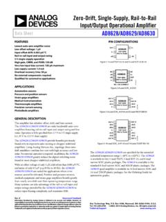
Transcription of AD708 Ultralow Offset Voltage Dual Op Amp (REV. C)
1 Ultralow Offset Voltage dual Op Amp Data Sheet AD708 Rev. D Document Feedback Information furnished by analog devices is believed to be accurate and reliable. However, no responsibility is assumed by analog devices for its use, nor for any infringements of patents or other rights of third parties that may result from its use. Specifications subject to change without notice. No license is granted by implication or otherwise under any patent or patent rights of analog devices . Trademarks and registered trademarks are the property of their respective owners. One Technology Way, Box 9106, Norwood, MA 02062-9106, Tel: 2018 analog devices , Inc. All rights reserved. Technical Support FEATURES Very high dc precision 30 V maximum Offset Voltage V/ C maximum Offset Voltage drift V p-p maximum Voltage noise ( Hz to 10 Hz) 5 million V/V minimum open-loop gain 130 dB minimum CMRR 120 dB minimum PSRR Matching characteristics 30 V maximum Offset Voltage match V/ C maximum Offset Voltage drift match 130 dB minimum CMRR match Available in 8-lead narrow body, PDIP, and hermetic CERDIP and CERDIP/883B packages PIN CONFIGURATION 1 OUTPUT A2 IN A3+IN A4 VS+VS8 OUTPUT B7 IN B6+IN B5AD708 TOP VIEW(Not to Scale)A + +B05789-001 Figure 1.
2 PDIP (N) and CERDIP (Q) Packages GENERAL DESCRIPTION The AD708 is a high precision, dual monolithic operational amplifier. Each amplifier individually offers excellent dc precision with maximum Offset Voltage and Offset Voltage drift of any dual bipolar op amp. The matching specifications are among the best available in any dual op amp. In addition, the AD708 provides 5 V/ V mini-mum open-loop gain and guaranteed maximum input Voltage noise of 350 nV p-p ( Hz to 10 Hz). All dc specifications show excellent stability over temperature, with Offset Voltage drift typically V/ C and input bias current drift of 25 pA/ C maximum. The AD708 is available in four performance grades. The AD708J is rated over the commercial temperature range of 0 C to 70 C and is available in a narrow body, PD I P.
3 T h e AD708A and AD708B are rated over the industrial temperature range of 40 C to +85 C and are available in a C E R D I P. The AD708S is rated over the military temperature range of 55 C to +125 C and is available in a CERDIP military version processed to MIL-STD-883B. PRODUCT HIGHLIGHTS 1. The combination of outstanding matching and individual specifications make the AD708 ideal for constructing high gain, precision instrumentation amplifiers. 2. The low Offset Voltage drift and low noise of the AD708 allow the designer to amplify very small signals without sacrificing overall system performance. 3. The AD708 10 V/ V typical open-loop gain and 140 dB common-mode rejection make it ideal for precision applications. AD708 Data Sheet Rev.
4 D | Page 2 of 16 TABLE OF CONTENTS Features .. 1 Pin Configuration .. 1 General Description .. 1 Product Highlights .. 1 Revision History .. 2 Specifications .. 3 Absolute Maximum Ratings .. 5 ESD Caution .. 5 Typical Performance Characteristics .. 6 Matching Characteristics .. 9 Theory of Operation .. 10 Crosstalk Performance .. 10 Operation with a Gain of 100 .. 11 High Precision Programmable Gain Amplifier .. 11 Bridge Signal 12 Precision Absolute Value Circuit .. 12 Selection of Passive Components .. 12 Outline Dimensions .. 13 Ordering Guide .. 13 REVISION HISTORY 7/2018 Rev. C to Rev. D Changes to Figure 28, Figure 29, and High Precision Programmable Gain Amplifier Section .. 11 Changes to Ordering Guide .. 13 1/2006 Rev. B to Rev.
5 C Updated Format .. Universal Removed TO-99 Package .. Universal Deleted AD707 References .. Universal Deleted LT1002 1 Deleted Figure 1 .. 1 Deleted Metalization Photograph .. 5 Moved Figure 25, Figure 26, and Figure 27 to Theory of Operation section .. 10 Updated Outline Dimensions .. 13 Changes to Ordering Guide .. 13 2/1991 Rev. A to Rev. B Data Sheet AD708 Rev. D | Page 3 of 16 SPECIFICATIONS At 25 C and 15 V dc, unless otherwise noted. Table 1. AD708J/AD708A AD708B AD708S Parameter Conditions Min1 Typ Max1 Min1 Typ Max1 Min1 Typ Max1 Unit INPUT Offset VOLTAGE2 30 100 5 50 5 30 V TMIN to TMAX 50 150 15 65 15 50 V Drift V/ C Long Term Stability V/month INPUT BIAS CURRENT 1 nA TMIN to TMAX 4 nA Average Drift 15 40 10 25 10 30 pA/ C Offset CURRENT VCM = 0 V 1 nA TMIN to TMAX nA Average Drift 2 60 1 25 1 25 pA/ C MATCHING CHARACTERISTICS3 Offset Voltage 80 50 30 V TMIN to TMAX 150 75 50 V Offset Voltage Drift V/ C Input Bias Current nA TMIN to TMAX nA
6 Common-Mode Rejection 120 140 130 140 130 140 dB TMIN to TMAX 110 130 130 dB Power Supply Rejection 110 120 120 dB TMIN to TMAX 110 120 120 dB Channel Separation 135 140 140 dB INPUT Voltage NOISE Hz to 10 Hz V p-p f = 10 Hz 18 12 12 nV/ Hz f = 100 Hz 11 nV/ Hz f = 1 kHz 11 nV/ Hz INPUT CURRENT NOISE Hz to 10 Hz 14 35 14 35 14 35 pA p-p f = 10 Hz pA/ Hz f = 100 Hz pA/ Hz f = 1 kHz pA/ Hz COMMON-MODE REJECTION R AT I O VCM = 13 V 120 140 130 140 130 140 dB TMIN to TMAX 120 140 130 140 130 140 dB OPEN-LOOP GAIN VO = 10 V RLOAD 2 k 3 10 5 10 4 10 V/ V TMIN to TMAX 3 10 5 10 4 7 V/ V POWER SUPPLY REJECTION R AT I O VS = 3 V to 18 V 110 130 120 130 120 130 dB TMIN to TMAX 110 130 120 130 120 130 dB FREQUENCY RESPONSE Closed-Loop Bandwidth MHz Slew Rate V/ s INPUT RESISTANCE Differential 60 200 200 M Common Mode 200 400 400 G AD708 Data Sheet Rev.
7 D | Page 4 of 16 AD708J/AD708A AD708B AD708S Parameter Conditions Min1 Typ Max1 Min1 Typ Max1 Min1 Typ Max1 Unit OUTPUT Voltage RLOAD 10 k 14 14 V RLOAD 2 k 13 V RLOAD 1 k V TMIN to TMAX 13 V OPEN-LOOP OUTPUT RESISTANCE 60 60 60 POWER SUPPLY Quiescent Current mA Power Consumption VS = 15 V 135 165 135 165 135 165 mW VS = 3 V 12 18 12 18 12 18 mW Operating Range 3 18 3 18 3 18 V 1 All min and max specifications are guaranteed. Specifications in boldface are tested on all production units at final electrical test. Results from those tests are used to calculate outgoing quality levels.
8 2 Input Offset Voltage specifications are guaranteed after five minutes of operation at TA = 25 C. 3 Matching is defined as the difference between parameters of the two amplifiers. Data Sheet AD708 Rev. D | Page 5 of 16 ABSOLUTE MAXIMUM RATINGS Table 2. Parameter Rating Supply Voltage 22 V Internal Power Dissipation1 Input Voltage2 VS Output Short-Circuit Duration Indefinite Differential Input Voltage +VS and VS Storage Temperature Range (Q) 65 C to +150 C Storage Temperature Range (N) 65 C to +125 C Lead Temperature (Soldering 60 sec) 300 C 1 Thermal Characteristics 8-lead PDIP: JC = 33 C/W, JA = 100 C/W 8-lead CERDIP: JC = 30 C/W, JA = 110 C/W 2 For supply voltages less than 22 V, the absolute maximum input Voltage is equal to the supply Voltage .
9 Stresses at or above those listed under Absolute Maximum Ratings may cause permanent damage to the product. This is a stress rating only; functional operation of the product at these or any other conditions above those indicated in the operational section of this specification is not implied. Operation beyond the maximum operating conditions for extended periods may affect product reliability. ESD CAUTION AD708 Data Sheet Rev. D | Page 6 of 16 TYPICAL PERFORMANCE CHARACTERISTICS VS = 15 V and TA = 25 C, unless otherwise noted. +VS+V V Voltage LIMIT (V)(REFERRED TO SUPPLY VOLTAGES)SUPPLY Voltage ( V) Figure 2. Input Common-Mode Range vs. Supply Voltage +VS Voltage SWING ( V)(REFERRED TO SUPPLY VOLTAGES)SUPPLY Voltage ( V)+VOUT VOUTRL = 10k RL = 2k Figure 3.
10 Output Voltage Swing vs. Supply Voltage 35051015202530101001k10k05789-004 OUTPUT Voltage (V p-p)LOAD RESISTANCE ( ) 15V SUPPLIES Figure 4. Output Voltage Swing vs. Load Resistance 8701234560242118151296305789-005 SUPPLY CURRENT (mA)SUPPLY Voltage ( V) Figure 5. Supply Current vs. Supply Voltage 1009080706050403020100 OF UNITSOFFSET Voltage DRIFT ( V/ C)256 UNITS TESTED 55 C TO +125 C Figure 6. Typical Distribution of Offset Voltage Drift = +110k1k10010105789-007 OUTPUT IMPEDANCE ( )FREQUENCY (Hz)AV = +1000IO = 1mA Figure 7. Output Impedance vs. Frequency Data Sheet AD708 Rev. D | Page 7 of 16 4001020303551525011010005789-008 INVERTING OR NONINVERTING INPUTBIAS CURRENT (mA)DIFFERENTIAL Voltage ( V) Figure 8. Input Bias Current vs.
