Transcription of AD7641 18-Bit, 2 MSPS SAR ADC Data Sheet (Rev. 0)
1 18-Bit, 2 msps sar adc AD7641 Rev. A Information furnished by analog devices is believed to be accurate and reliable. However, no responsibility is assumed by analog devices for its use, nor for any infringements of patents or other rights of third parties that may result from its use. Specifications subject to change without notice. No license is granted by implication or otherwise under any patent or patent rights of analog devices . Trademarks and registered trademarks are the property of their respective owners. One Technology Way, Box 9106, Norwood, MA 02062-9106, Tel: Fax: 2006 2020 analog devices , Inc. All rights reserved. FEATURES Throughput 2 MSPS (wideband warp and warp mode) MSPS (normal mode) INL: 2 LSB typical, 3 LSB max; 8 ppm of full scale 18-bit resolution with no missing codes Dynamic range: dB SNR: dB typical @ 20 kHz (VREF = V) THD: 112 dB typical @ 20 kHz (VREF = V) V internal reference: typ drift 10 ppm/ C.
2 TEMP output Differential input range: VREF (VREF up to V) No pipeline delay (SAR architecture) Parallel (18-, 16-, or 8-bit bus) and serial 5 V interface SPI /QSPI /MICROWIRE /DSP compatible Single V supply operation Power dissipation 75 mW typical @ 2 MSPS with internal REF 2 W in power-down mode Pb-free, 48-lead LQFP and 48-lead LFCSP Speed upgrade of the AD7674, AD7678, AD7679 APPLICATIONS Medical instruments High speed data acquisition/high dynamic data acquisition Digital signal processing Spectrum analysis Instrumentation Communications ATE GENERAL DESCRIPTION The AD7641 is an 18-bit, 2 MSPS, charge redistribution SAR, fully differential, analog -to-digital converter (ADC) that operates from a single V power supply. The part contains a high speed, 18-bit sampling ADC, an internal conversion clock, an internal reference (and buffer), error correction circuits, and both serial and parallel system interface ports.
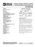
3 It features two very high sampling rate modes (wideband warp and warp) and a fast mode (normal) for asynchronous rate applications. The AD7641 is hardware factory calibrated and tested to ensure ac parameters, such as signal-to-noise ratio (SNR), in addition to the more traditional dc parameters of gain, offset, and linearity. The AD7641 is available in Pb-free only packages with operation specified from 40 C to +85 C. FUNCTIONAL BLOCK DIAGRAM 04761-00118 CONTROL LOGIC ANDCALIBRATION CIRCUITRYCLOCKAD7641 DGNDDVDDAVDDAGNDREFREFGNDIN+IN PDRESETCNVSTPDBUFREFBUFINPDREFREFTEMPD[1 7:0]BUSYRDCSD0/OB/2 COGNDOVDDMODE1 MODE0 REFAMPNORMALSERIALPORTPARALLELINTERFACES WITCHEDCAPDACWARP Figure 1. Table 1. PulSAR Selection Type/kSPS 100 to 250 500 to 570 650 to 1000 >1000 Pseudo Differential AD7651, AD7660, AD7661 AD7650, AD7652, AD7664, AD7666 AD7653, AD7667 True Bipolar AD7610, AD7663 AD7665 AD7612, AD7671 True Differential AD7675 AD7676 AD7677 AD7621, AD7622, AD7623 18-Bit Multichannel/ AD7631, AD7678 AD7679 AD7634, AD7674 AD7641 , AD7643 Simultaneous AD7654 AD7655 PRODUCT HIGHLIGHTS 1.
4 Fast Throughput. The AD7641 is a 2 MSPS, charge redistribution, 18-bit SAR ADC. 2. Superior Linearity. The AD7641 has no missing 18-bit code. 3. Internal Reference. The AD7641 has a V internal reference with a typical drift of 10 ppm/ C and an on-chip TEMP sensor. 4. Single-Supply Operation. The AD7641 operates from a V single supply. 5. Serial or Parallel Interface. Versatile parallel (16- or 8-bit bus) or 2-wire serial interface arrangement compatible with V, V, or 5 V logic. AD7641 Rev. A | Page 2 of 29 TABLE OF CONTENTS Features .. 1 Applications .. 1 General Description .. 1 Functional Block Diagram .. 1 Product Highlights .. 1 Revision History .. 2 Specifications .. 3 Timing Specifications .. 5 Absolute Maximum Ratings .. 7 ESD 7 Pin Configuration and Function Descriptions .. 8 Terminology .. 12 Typical Performance Characteristics .. 13 Appplications Information.
5 16 Circuit Information .. 16 Converter Operation .. 16 Modes of Operation .. 16 Transfer Functions .. 17 Typical Connection Diagram .. 18 analog Inputs .. 18 Multiplexed Inputs .. 18 Driver Amplifier Choice .. 18 Voltage Reference Input .. 19 Power Supply .. 21 Conversion Control .. 21 Interfaces .. 22 Digital Interface .. 22 Parallel Interface .. 22 Serial interface .. 23 Master Serial Interface .. 23 Slave Serial Interface .. 25 Microprocessor Interfacing .. 27 Application Hints .. 28 Layout .. 28 Evaluating the AD7641 Performance .. 28 Outline Dimensions .. 29 Ordering Guide .. 29 REVISION HISTORY 8/ 2020 Rev. 0 to Rev. A Changed CP-48-1 to CP-48-4 .. Throughout Added Figure 4; Renumbered Sequentially .. 8 Updated Outline Dimensions .. 28 Changes to Ordering Guide .. 28 1/2006 Revision 0: Initial Version AD7641 Rev. A | Page 3 of 29 SPECIFICATIONS AVDD = DVDD = V; OVDD = V to V; VREF = V; all specifications TMIN to TMAX, unless otherwise noted.
6 Table 2. Parameter Conditions Min Typ Max Unit RESOLUTION 18 Bits analog INPUT Voltage Range VIN+ VIN VREF +VREF V Operating Input Voltage VIN+, VIN to AGND AVDD1 V analog Input CMRR fIN = 100 kHz 58 dB Input Current 2 MSPS throughput 18 A Input Impedance2 THROUGHPUT SPEED Complete Cycle Wideband warp, warp modes 500 ns Throughput Rate Wideband warp, warp modes 2 MSPS Time Between Conversions Wideband warp, warp modes 1 ms Complete Cycle Normal mode 667 ns Throughput Rate Normal mode 0 MSPS DC ACCURACY Integral Linearity Error3 TMIN to TMAX = 40 C to +70 C 3 2 +3 LSB4 Integral Linearity Error TMIN to TMAX = 40 C to +85 C 2 + LSB4 No Missing Codes 18 Bits Differential Linearity Error 1 +2 LSB Transition Noise VREF = V LSB Transition Noise VREF = V LSB Zero Error, TMIN to TMAX5 15 +15 LSB Zero Error Temperature Drift ppm/ C Gain Error, TMIN to TMAX5 + % of FSR Gain Error Temperature Drift 1 ppm/ C Power Supply Sensitivity AVDD = V 5% 16 LSB AC ACCURACY Dynamic Range VREF = V dB6 Signal-to-Noise fIN = 20 kHz, VREF = V dB fIN = 20 kHz, VREF = V 92 dB fIN = 100 kHz, VREF = V 93 dB Spurious-Free Dynamic Range fIN = 20 kHz, VREF = V 112 dB fIN = 20 kHz, VREF = V 113 dB fIN = 100 kHz, VREF = V 101 dB Total Harmonic Distortion fIN = 20 kHz, VREF = V 115 dB fIN = 20 kHz, VREF = V 116 dB fIN = 100 kHz, VREF = V 101 dB Signal-to-(Noise + Distortion)
7 FIN = 20 kHz, , VREF = V dB fIN = 20 kHz, VREF = V 92 dB fIN = 100 kHz, , VREF = V dB 3 dB Input Bandwidth 50 MHz SAMPLING DYNAMICS Aperture Delay 1 ns Aperture Jitter 5 ps rms Transient Response Full-scale step 115 ns INTERNAL REFERENCE PDREF = PDBUF = low Output Voltage REF @ 25 C V Temperature Drift 40 C to +85 C 10 ppm/ C AD7641 Rev. A | Page 4 of 29 Parameter Conditions Min Typ Max Unit Line Regulation AVDD = V 5% 15 ppm/V Turn-On Settling Time CREF = 10 F 5 ms REFBUFIN Output Voltage REFBUFIN @ 25 C V REFBUFIN Output Resistance k EXTERNAL REFERENCE PDREF = PDBUF = high Voltage Range REF AVDD + V Current Drain 2 MSPS throughput 180 A REFERENCE BUFFER PDREF = high, PDBUF = low REFBUFIN Input Voltage Range REF = V typ V REFBUFIN Input Current REFBUFIN = V 1 nA TEMPERATURE PIN Voltage Output @ 25 C 278 mV Temperature Sensitivity 1 mV/ C Output Resistance k DIGITAL INPUTS Logic Levels VIL + V VIH V IIL 1 +1 A IIH 1 +1 A DIGITAL OUTPUTS Data Format7 Pipeline Delay8 VOL ISINK = 500 A V VOH ISOURCE = 500 A OVDD V POWER SUPPLIES Specified Performance AVDD V DVDD V OVDD V Operating Current10 2 MSPS throughput AVDD11 With internal reference 23 mA DVDD mA OVDD12 mA Power Dissipation11 With Internal Reference10 2 MSPS throughput 75 92 mW Without Internal Reference10 2 MSPS throughput 68 85 mW In Power-Down Mode12 PD = high 2 W TEMPERATURE RANGE13 Specified Performance TMIN to TMAX 40 +85 C 1 When using
8 An external reference. With the internal reference, the input range is V to VREF. 2 See analog Inputs section. 3 Linearity is tested using endnotes, not best fit. 4 LSB means least significant bit. With the V input range, 1 LSB is V. 5 See Voltage Reference Input section. These specifications do not include the error contribution from the external reference. 6 All specifications in dB are referred to a full-scale input FS. Tested with an input signal at dB below full-scale, unless otherwise specified. 7 Parallel or serial 18-bit. 8 Conversion results are available immediately after completed conversion. 9 See the Absolute Maximum Ratings section. 10 In warp mode. Tested in parallel reading mode. 11 With internal reference, PDREF and PDBUF are low; without internal reference, PDREF and PDBUF are high. 12 With all digital inputs forced to OVDD. 13 Consult sales for extended temperature range.
9 AD7641 Rev. A | Page 5 of 29 TIMING SPECIFICATIONS AVDD = DVDD = V; OVDD = V to V; VREF = V; all specifications TMIN to TMAX, unless otherwise noted. Table 3. Parameter Symbol Min Typ Max Unit CONVERSION AND RESET (Refer to Figure 30 and Figure 31) Convert Pulse Width t1 15 701 ns Time Between Conversions (Warp Mode2/Normal Mode3) t2 500/667 ns CNVST Low to BUSY High Delay t3 23 ns BUSY High All Modes (Except Master Serial Read After Convert) t4 385/520 ns Aperture Delay t5 1 ns End of Conversion to BUSY Low Delay t6 10 ns Conversion Time (Warp Mode/Normal Mode) t7 385/520 ns Acquisition Time (Warp Mode/Normal Mode) t8 115 ns RESET Pulse Width t9 15 ns RESET Low to BUSY High Delay4 t38 10 ns BUSY High Time from RESET Low4 t39 600 ns PARALLEL INTERFACE MODES (Refer to Figure 32 to Figure 35 ) CNVST Low to Data Valid Delay (Warp Mode/Normal Mode)
10 T10 385/520 ns Data Valid to BUSY Low Delay t11 2 ns Bus Access Request to Data Valid t12 20 ns Bus Relinquish Time t13 2 15 ns MASTER SERIAL INTERFACE MODES5 (Refer to Figure 36 and Figure 37) CS Low to SYNC Valid Delay t14 10 ns CS Low to Internal SCLK Valid Delay5 t15 10 ns CS Low to SDOUT Delay t16 10 ns CNVST Low to SYNC Delay (Warp Mode/Normal Mode) t17 14/137 ns SYNC Asserted to SCLK First Edge Delay t18 ns Internal SCLK Period6 t19 8 14 ns Internal SCLK High6 t20 2 ns Internal SCLK Low6 t21 3 ns SDOUT Valid Setup Time6 t22 1 ns SDOUT Valid Hold Time6 t23 0 ns SCLK Last Edge to SYNC Delay6 t24 0 ns CS High to SYNC HI-Z t25 10 ns CS High to Internal SCLK HI-Z t26 10 ns CS High to SDOUT HI-Z t27 10 ns BUSY High in Master Serial Read After Convert6 t28 See Table 4 ns CNVST Low to SYNC Asserted Delay (All Modes) t29 383/500 ns SYNC Deasserted to BUSY Low Delay t30 13 ns SLAVE SERIAL INTERFACE MODES (Refer to Figure 39 and Figure 40) External SCLK Setup Time t31 5 ns External SCLK Active Edge to SDOUT Delay t32 1 8 ns SDIN Setup Time t33 5 ns SDIN Hold Time t34 5 ns External SCLK Period t35 ns External SCLK High t36 5 ns External SCLK Low t37 5 ns 1 See the Conversion Control section.