Transcription of AD87588 - Micro Bridge
1 ESMT AD87588 Elite Semiconductor Memory Technology Inc. Publication Date: Feb. 2015 Revision: 1/68 2x20W stereo / 1x40W Mono Digital audio amplifier With 20 Bands EQ Functions + Capless Line Driver Features z 16/18/20/24-bits input with I2S, Left-alignment and Right-alignment data format z PSNR & DR(A-weighting) Loudspeaker: 97dB (PSNR), 105dB (DR) @24V z Multiple sampling frequencies (Fs) 32kHz / / 48kHz and 64kHz / / 96kHz and 128kHz / / 192kHz z System clock = 64x, 128x, 192x, 256x, 384x, 512x, 576x, 768x, 1024x Fs 64x~1024x Fs for 32kHz / / 48kHz 64x~512x Fs for 64kHz / / 96kHz 64x~256x Fs for 128kHz / / 192kHz z Supply voltage for digital circuit 10V~26V for loudspeaker driver z Loudspeaker output power for stereo @24V 10W x 2ch into 8 THD+N 15W x 2ch into 8 THD+N 20W x 2ch into 8 THD+N z Loudspeaker output power for Mono@24V 20W x 1ch into 8 THD+N 30W x 1ch into 8 THD+N 40W x 1ch into 8 THD+N z Sound processing including 20 bands parametric speaker EQ Volume control (+24dB~-103dB, ), Dynamic range control (DRC)
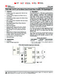
2 Dual band dynamic range control Power clipping 3D surround sound Channel mixing Noise gate with hysteresis window Bass/Treble tone control Bass management crossover filter DC-blocking high-pass filter z Anti-pop design z Short circuit and over-temperature protection z I2C control interface with selectable device address z Support hardware and software reset z Internal PLL z LV Under-voltage shutdown and HV Under-voltage detection z Power saving mode z Support initial EEPROM setting Applications z TV audio z Boom-box, CD and DVD receiver, docking system z Powered speaker z Wireless audio Description The AD87588 is an integrated audio system solution, embedding digital audio process, power stage amplifier , and a stereo 3 Vrms line driver. AD87588 is a digital audio amplifier capable of driving a pair of 8 , 20W or a single 4 , 40W operating at 24V supply. AD87588 is also capable of driving 4 , 10W (SE)x2 + 8 , 20W (BTL)x1 at 24V supply for application.
3 AD87588 can provide advanced audio processing capabilities, such as volume control, 20 bands speaker EQ, audio mixing, 3D surround and Dynamic Range Control (DRC). These functions are fully programmable via a simple I2C control interface. Robust protection circuits are provided to protect AD87588 from damage due to accidental erroneous operating condition. AD87588 is more tolerant to noise and PVT (Process, Voltage, and Temperature) variation than the analog Class-AB or Class-D audio amplifier counterpart implemented by analog circuit design. AD87588 is pop free during instantaneous power switch because of its built-in, robust anti-pop circuit. ESMT AD87588 Elite Semiconductor Memory Technology Inc. Publication Date: Feb. 2015 Revision: 2/68 Pin Assignment MCLKDGNDDVDDSDATA03635343332313029282726 25123456789101112 DVDDDGNDSDAPDERRORRESETCFG0 CLK_OUTPLLCFG1 BCLKLRCINSCLSA0SA1 DEFLREXMSSDATA1 LINEIN Pin Description PIN NAME TYPE DESCRIPTION CHARACTERISTICS 1 SDATA1 I Serial audio data input 1 Schmitt trigger TTL input buffer 2 MS I EEPROM selection Schmitt trigger TTL input buffer 3 PLL I PLL enable, low active Schmitt trigger TTL input buffer 4 CFG0 I stereo / configuration pin Schmitt trigger TTL input buffer 5 CFG1 I stereo / configuration pin Schmitt trigger TTL input buffer 6 CLK_OUT O Clock output from PLL TTL output buffer 7 DGND P Digital Ground ( ) 8 DVDD P Digital Power ( ) 9 SDATA0 I Serial audio data input 0 Schmitt trigger TTL input buffer 10 LRCIN I Left/Right clock input (Fs) Schmitt trigger TTL input buffer 11 BCLK I Bit clock input (64Fs)
4 Schmitt trigger TTL input buffer 12 MCLK I Master clock input Schmitt trigger TTL input buffer 13 RINN I Right input for line driver 14 ROUT O Right output for line driver 15 SGND P Ground for line driver 16 EN I Enable for line driver 17 PVSS P Supply voltage for line driver 18 CN IO Charge pump flying capacitor negative connection for line driver ESMT AD87588 Elite Semiconductor Memory Technology Inc. Publication Date: Feb. 2015 Revision: 3/68 19 CP IO Charge pump flying capacitor positive connection for line driver 20 PVDD P Supply voltage for line driver 21 PGND P Ground for line driver 22 UVP I Under voltage protection for line driver 23 LOUT O Left output for Line driver 24 LINN I Left input for Line driver 25 SDA I/O I2C bi-directional serial data Schmitt trigger TTL input buffer 26 SCL I/O I2C serial clock input Schmitt trigger TTL input buffer 27 SA0 I I2C select address 0 Schmitt trigger TTL input buffer 28 SA1 I I2C select address 1 Schmitt trigger TTL input buffer 29 DEF I Initial default volume setting (1:Un-Mute.)
5 0:Mute) Schmitt trigger TTL input buffer 30 DGND P Digital Ground ( ) 31 DVDD P Digital Power ( ) 32 PD I Power down, low active Schmitt trigger TTL input buffer 33 ERROR O Error status, low active Open-drain output 34 RESET I Reset, low active Schmitt trigger TTL input buffer 35 LREX I Left/Right channel exchange (0:Unchanged ; 1:Exchanged) Schmitt trigger TTL input buffer 36 LINEIN I Select input data (0:SDATA0 ; 1:SDATA1) Schmitt trigger TTL input buffer 37 38 VDDRA P Right channel supply A 39 RA O Right channel output A 40 GNDR P Right channel ground 41 RB O Right channel output B 42 VDDRB P Right channel supply B 43 VDDLB P Left channel supply B 44 LB O Left channel output B 45 GNDL P Left channel ground 46 LA O Left channel output A 47 VDDLA P Left channel supply A 48