Transcription of AD9221/AD9223/AD9220 Complete 12-Bit 1.5 ... - Analog …
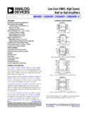
1 REV. EInformation furnished by Analog Devices is believed to be accurate andreliable. However, no responsibility is assumed by Analog Devices for itsuse, nor for any infringements of patents or other rights of third parties thatmay result from its use. No license is granted by implication or otherwiseunder any patent or patent rights of Analog Devices. Trademarks andregistered trademarks are the property of their respective Technology Way, Box 9106, Norwood, MA 02062-9106, : 781/329-4700 : 781/326-8703 2003 Analog Devices, Inc. All rights 12-Bit MSPSM onolithic A/D ConvertersFEATURESM onolithic 12-Bit A/D Converter Product FamilyFamily Members Are: AD9221, AD9223, and AD9220 Flexible Sampling Rates: MSPS, MSPS, MSPSLow Power Dissipation: 59 mW, 100 mW, and 250 mWSingle 5 V SupplyIntegral Nonlinearity Error: LSBD ifferential Nonlinearity Error: LSBI nput Referred Noise: LSBC omplete On-Chip Sample-and-Hold Amplifier andVoltage ReferenceSignal-to-Noise and Distortion Ratio: 70 dBSpurious-Free Dynamic Range.
2 86 dBOut-of-Range IndicatorStraight Binary Output Data28-Lead SOIC and 28-Lead SSOPFUNCTIONAL BLOCK DIAGRAMVINACAPTCAPBSENSEOTRBIT 1(MSB)BIT 12(LSB)VREFDVSSAVSSCMLAD9221/AD9223/AD92 20 SHADIGITAL CORRECTION LOGICOUTPUT BUFFERSVINB1 VREFCOM554433312 DVDDAVDDCLKMODESELECTMDAC3 GAIN = 4 MDAC2 GAIN = 8 MDAC1 GAIN = 16A/DA/DA/DA/DGENERAL DESCRIPTIONThe AD9221, AD9223, and AD9220 are a generation of highperformance, single supply 12-Bit Analog -to- digital device exhibits true 12-Bit linearity and temperature driftperformance1 as well as or better ac TheAD9221/AD9223/AD9220 share the same interface options,package, and pinout. Thus, the product family provides an upwardor downward component selection path based on performance,sample rate and power.
3 The devices differ with respect to theirspecified sampling rate, and power consumption, which is reflectedin their dynamic performance over AD9221/AD9223/AD9220 combine a low cost, high speedCMOS process and a novel architecture to achieve the resolutionand speed of existing hybrid and monolithic implementations ata fraction of the power consumption and cost. Each device is acomplete, monolithic ADC with an on-chip, high performance,low noise sample-and-hold amplifier and programmable voltagereference. An external reference can also be chosen to suit thedc accuracy and temperature drift requirements of the devices use a multistage differential pipelined architecturewith digital output error correction logic to provide 12-Bit accu-racy at the specified data rates and to guarantee no missingcodes over the full operating temperature input of the AD9221/AD9223/AD9220 is highly flexible,allowing for easy interfacing to imaging, communications, medi-cal, and data -acquisition systems.
4 A truly differential inputstructure allows for both single-ended and differential inputinterfaces of varying input spans. The sample-and-holdamplifier (SHA) is equally suited for both multiplexed sys-tems that switch full-scale voltage levels in successive channelsas well as sampling single-channel inputs at frequencies up toand beyond the Nyquist rate. Also, the AD9221/AD9223/AD9220is well suited for communication systems employing Direct-IF down conversion since the SHA in the differential inputmode can achieve excellent dynamic performance far beyond itsspecified Nyquist single clock input is used to control all internal conversioncycles. The digital output data is presented in straight binaryoutput format. An out-of-range (OTR)
5 Signal indicates an over-flow condition that can be used with the most significant bit todetermine low or high HIGHLIGHTSThe AD9221/AD9223/AD9220 family offers a Complete single-chip sampling 12-Bit , Analog -to- digital conversion function inpin compatible 28-lead SOIC and SSOP Sampling Rates The AD9221, AD9223, and AD9220offer sampling rates of MSPS, MSPS, and MSPS, Power and Single Supply The AD9221, AD9223, andAD9220 consume only 59 mW, 100 mW, and 250 mW, respec-tively, on a single 5 V power DC Performance Over Temperature The AD9221/AD9223/AD9220 provide 12-Bit linearity and temperature AC Performance and Low Noise The AD9221/AD9223/AD9220 provide better than ENOB performanceand have an input referred noise of LSB Analog Input Range The versatile on-board sample-and-hold (SHA) can be configured for either single-ended ordifferential inputs of varying input internal voltage on the Analog input E 2 AD9221/AD9223/AD9220 SPECIFICATIONS(AVDD = 5 V, DVDD = 5 V, fSAMPLE = Max Conversion Rate, VREF = V, VINB = V, TMIN to TMAX, unlessotherwise noted.)
6 ParameterAD9221AD9223AD9220 UnitRESOLUTION121212 Bits minMAX CONVERSION minINPUT REFERRED NOISE (TYP)VREF = 1 rms typVREF = rms typACCURACYI ntegral Nonlinearity (INL) typ maxDifferential Nonlinearity (DNL) typ maxINL1 typDNL1 typNo Missing Codes121212 Bits GuaranteedZero Error (@ 25 C) FSR maxGain Error (@ 25 C)2 FSR maxGain Error (@ 25 C)3 FSR maxTEMPERATURE DRIFTZero Error 2 2 2ppm/ C typGain Error2 26 26 26ppm/ C typGain Error3 C typPOWER SUPPLY REJECTIONAVDD, DVDD (+5 V V) FSR maxANALOG INPUTI nput Span (with VREF = V)222V p-p minInput Span (with VREF = V)555V p-p maxInput (VINA or VINB) Range000V minAVDDAVDDAVDDV maxInput Capacitance161616pF typINTERNAL VOLTAGE REFERENCEO utput Voltage (1 V Mode)111V typOutput Voltage Tolerance (1 V Mode) 14 14 14mV maxOutput Voltage ( V Mode) typOutput Voltage Tolerance ( V Mode) 35 35 35mV maxLoad maxREFERENCE INPUT RESISTANCE555k typPOWER SUPPLIESS upply VoltagesAVDD555V ( 5% AVDD Operating) to to to < typPOWER maxNOTES1 VREF = 1 internal internal regulation with 1 mA load current (in addition to that required by the AD9221/AD9223/AD9220 ).
7 Specification subject to change without SPECIFICATIONSREV. EAD9221/AD9223/AD9220 3 AC SPECIFICATIONS(AVDD = 5 V, DVDD= 5 V, fSAMPLE = Max Conversion Rate, VREF = V, VINB = V, DC Coupled/Single-Ended Input TMIN to TMAX, unless otherwise noted.)ParameterAD9221AD9223AD9220 UnitMAX CONVERSION minDYNAMIC PERFORMANCE Input Test Frequency 1 (VINA = dBFS)1005001000kHzSignal-to-Noise and Distortion (SINAD) minEffective Number of Bits (ENOBs) minSignal-to-Noise Ratio (SNR) minTotal Harmonic Distortion (THD) typ maxSpurious Free Dynamic Range (SFDR) maxInput Test Frequency 2 (VINA = dBFS) and Distortion (SINAD) minEffective Number of Bits (ENOBs) minSignal-to-Noise Ratio (SNR) minTotal Harmonic Distortion (THD) typ maxSpurious Free Dynamic Range (SFDR)
8 MaxFull Power Bandwidth254060 MHz typSmall Signal Bandwidth254060 MHz typAperture Delay111ns typAperture Jitter444ps rms typAcquisition to Full-Scale Step1254330ns typSpecifications subject to change without SPECIFICATIONS(AVDD = 5 V, DVDD = 5 V, TMIN to TMAX, unless otherwise noted.)ParameterSymbol UnitCLOCK INPUTHigh Level Input minLow Level Input maxHigh Level Input Current (VIN = DVDD)IIH 10 A maxLow Level Input Current (VIN = 0 V)IIL 10 A maxInput CapacitanceCIN5pF typLOGIC OUTPUTSDVDD = 5 V High Level Output Voltage (IOH = 50 A) min High Level Output Voltage (IOH = mA) min Low Level Output Voltage (IOL = mA) max Low Level Output Voltage (IOL = 50 A) maxDVDD = 3 V High Level Output Voltage (IOH = 50 A) min High Level Output Voltage (IOH = mA) min Low Level Output Voltage (IOL = mA) max Low Level Output Voltage (IOL = 50 A)
9 MaxOutput CapacitanceCOUT5pF typSpecifications subject to change without E 4 AD9221/AD9223/AD9220 SWITCHING SPECIFICATIONS(TMIN to TMAX with AVDD = 5 V, DVDD = 5 V, CL = 20 pF)ParameterSymbolAD9221AD9223AD9220 UnitClock Period*tC667333100ns minCLOCK Pulsewidth HightCH30015045ns minCLOCK Pulsewidth LowtCL30015045ns minOutput DelaytOD888ns min131313ns typ191919ns maxPipeline Delay (Latency)333 Clock Cycles*The clock period may be extended to 1 ms without degradation in specified performance @ 25 subject to change without notice. tCL tCH tCtODDATA 1 DATAOUTPUTINPUTCLOCKANALOGINPUTS1S2S3S4 Figure 1. Timing DiagramABSOLUTE MAXIMUM RATINGS*WithRespectParametertoMinMaxUnit AVDDAVSS + + + + + + VDigital OutputsDVSS + VVINA, VINBAVSS + VVREFAVSS + VSENSEAVSS + VCAPB, CAPTAVSS + VJunction Temperature150 CStorage Temperature 65+150 CLead Temperature(10 sec)300 C*Stresses above those listed under Absolute Maximum Ratings may cause perma-nent damage to the device.
10 This is a stress rating only; functional operation of thedevice at these or any other conditions above those indicated in the operationalsections of this specification is not implied. Exposure to absolute maximum ratingsfor extended periods may effect device CHARACTERISTICST hermal Resistance28-Lead SOIC JA = C/W JC = 23 C/W28-Lead SSOP JA = C/W JC = 23 C/WORDERING GUIDET emperaturePackagePackageModelRangeDescri ptionOptionAD9221AR 40 C to +85 C28-Lead SOICR-28AD9223AR 40 C to +85 C28-Lead SOICR-28AD9220AR 40 C to +85 C28-Lead SOICR-28AD9221 ARS 40 C to +85 C28-Lead SSOPRS-28AD9223 ARS 40 C to +85 C28-Lead SSOPRS-28AD9220 ARS 40 C to +85 C28-Lead SSOPRS-28AD9221-EBEvaluation BoardAD9223-EBEvaluation BoardAD9220-EBEvaluation BoardCAUTIONESD (electrostatic discharge) sensitive device.
