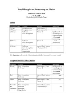
Transcription of Alternatives To HASL: Users Guide For Surface Finishes
1 Alternatives To hasl : Users Guide For Surface Finishes By Dan T. Parquet and David W. Boggs Merix Corporation, Forest Grove, OR INTRODUCTION A great deal of controversy continues to surround the use of Hot Air Solder Leveling ( hasl ) in the production of printed circuit boards (PCBs). The financial burden, technological limitations and environmental issues surrounding the hasl process continue to grow. This requires an in-depth review by the printed circuit board manufacturing plant, as well as the assembly operation and instrument designers ( OEMs), to determine what alternative Surface Finishes are appropriate. The benefits of hasl replacement are many. Let s examine them by category of user : Circuit Board Producer ??Eliminates lead and hazardous waste expense ??Eliminates safety issues: toxic fumes and fire hazards ??Reduces maintenance: 20 percent down time is common ??Reduces utility costs for heating of hot air and solder ?
2 ?Fine pitch technology improvement by eliminating bridging ??Improves yield ??Reduces rework Circuit Board Assembler ??Improves pad coplanarity for superior solder paste print accuracy and component placement ??Improves bare board cleanliness, or Surface Insulation Resistance (SIR) ??Less warp due to reduced thermal stress at producer ??Solder contrast aids solder joint inspection ??Reduces opens and shorts (bridging) with fine pitch devices Original Equipment Manufacturer ??Improves reliability from minimal copper-tin intermetallic formation ??Improves circuit density by the elimination of hole compensation ??Permits device attachment solder volume control ??Improves fine pitch design ability (removes board level hasl issues) A variety of Surface finish Alternatives to Hot Air Solder Leveling ( hasl ) exist that present the circuit designer, board fabricator, and component assembler with some interesting and challenging options.
3 Electrolytic tin, electroless nickel/immersion gold, and organic solderability preservatives (OSPs) are just a few that are available on the market. Of these possibilities, organic solderability preservatives, also known as anti-tarnish, are gaining popularity in the industry as low cost alternative to hasl . The OSP Surface finish satisfies assembly requirements for fine pitch, through hole, and mixed technology product. These coatings may be defined as a water-based organic compound that selectively bonds with copper to provide an organometallic layer that protects the copper. Electroless nickel/immersion gold satisfies application-specific requirements for ultra-fine pitch technology, wire bond ability, and superior contact resistance. This process is two-layer, gold over nickel metallic Surface finish plated onto the copper base by means of a chemical deposition process. Pure tin offers a distinct environmental advantage over the traditional lead bearing alloys used as temporary metal etch resists and final plated Surface Finishes .
4 Matte tin circuitry is a two-layer, tin over nickel metallic Surface finish plated onto the copper base by means of an electrolytic process. BACKGROUND Printed circuit boards requiring component attachment, whether leaded or Surface mount technology (SMT), must have the exposed copper land areas coated with a protective finish. This protective coating must be solderable and, at the same time, act as a barrier for preventing the copper from oxidizing which causes assembly problems for the end user . In the United States, the predominant Surface finish in the PCB industry is hasl . Driven by the push for Solder Mask Over Bare Copper (SMOBC), hasl was born as a reliable method to apply solder to the copper surfaces after solder mask. A thin layer of eutectic solder is deposited onto the exposed copper by passing the boards through a hot, molten wave (or pot) of solder and subsequently blasting the excess solder from the boards using high velocity hot air.
5 This process is currently under scrutiny due to environmental and safety issues (hazardous waste/lead exposure), technological limitations (fine-pitch device assembly), and equipment maintenance expenses to name a few. In contrast, the alternative processes are environmentally friendly, some provide a Surface planarity equivalent to the plated copper finish, and most require very low equipment maintenance. Organic Solderability Preservatives (OSP, Anti-tarnish) Of the OSP compounds, the two that are predominant in the industry are benzotriazole and substituted benzimidazole. The former of these has been utilized both in the metal finishing industry as a true anti-tarnish for hardware plating, and to a lesser degree, in the electronics industry for limited heat cycle solder applications on bare copper. The more recently developed substituted benzimidazole compounds have the advantage of withstanding multiple heat cycles typically found in mixed technology PCB assembly operations ( Surface mount and through hole soldering).
6 This advantage is primarily due to the coating thickness that is achieved with the substituted compounds, ranging from 5 to 20 microinches1 ( - microns), as compared to only a monomolecular layer formed with the benzotriazole materials. In general, OSPs are considered the low cost, high volume alternative, particularly when applied to Surface mount technology due to the excellent Surface coplanarity of pads. The cost advantage of the process becomes quite apparent to the board fabricator. For example, facilities and maintenance expenses are only a fraction of the operating cost for the anti-tarnish process as compared to hasl . The process does not involve heating and delivering the high volume air or maintaining a molten pot of solder. Losses due to rework and rejected product from the hasl process are substantial and prevent a decrease in the cost of manufacturing. An OSP application system eliminates this waste and allows for flexibility to pass the savings on to the customer.
7 The cost advantage to the assembler lies primarily in the yield improvements of the component attachment process. Surface mount pad planarity is a technical hurdle that hasl will never overcome, especially for fine pitch devices due to the extreme variation in coating thickness. This non-uniform solder thickness can range from 30-1500 microinches ( - microns) depending upon pad geometry and orientation within the panel. In contrast, an OSP coated board provides a Surface finish topography equivalent to the plated copper. This allows for improved component placement; furthermore, it will help move the assembler towards finer pitch devices and denser circuits as the limiting factor for fine pitch assembly now becomes the ability to deposit the solder paste. It must be emphasized that implementing an OSP process may require a re-characterization of the assembly operation; a number of issues must be addressed.
8 For example, the number of thermal cycles a product may see in the assembly process can reduce the operating window for soldering. If excessive, it may be determined that soldering in an inert atmosphere is required in the reflow process, wave solder, or both. Typically, OSP suppliers advertise up to five thermal cycles can be achieved in open air without detrimental effects to solderability. Developing a partnership with the board shop and supplier is an important consideration during the implementation phase. A second assembly process consideration when using OSP technology surrounds the type and activity of the flux used in each of the assembly operations. Table 1 illustrates the results of an engineering evaluation used to benchmark OSPs in comparison to hasl coated PCBs at one customer site. It was apparent in the evaluation that the OSPs performed differently depending upon the type of flux used.
9 A wide range of responses were found spanning from excellent Surface mount solderability with OA or RMA type solder pastes, to relatively poor filling of holes with a low solids (2%) no clean wave solder flux that was not designed for soldering to OSP coated pads. Assembly Operation SMT Paste Flux Type Wave Solder Flux Type Results with OSP Customer A Organic Acid (OA) Organic Acid (OA) Compatible with all processes Customer B Active Rosin (RMA) No Clean (2% solids Compatible with SMT process, Alternative No Clean wave flux required Customer C Active Rosin (RMA) Organic Acid (OA) Compatible with all processes Customer D N/A No Clean (2% solids) Alternate No Clean wave flux required Table 1 At the OEM level, the three key attributes that OSP technology provides the designer are solder joint reliability, circuit density latitude, and the ability to engineer solder joints. A standard hasl design rule, which is used in the tooling of PCBs, is to oversize drilled holes by " - " (50 - 150 microns) to compensate for the reduction in hole diameter caused by the non-uniform hasl solder deposit.)
10 With the use of an OSP, this compensation is not necessary; it allows for a reduction of pad size and an overall increase in circuit density. Additionally, since good solder wetting occurs only where the flux comes into contact with the OSP coated copper pad, the flow characteristics of the solder are more controlled. This reduces the risk of bridging and provides the possibility for predicting final solder volume. Electroless Nickel/Immersion Gold Electroless nickel is well known in the metal finishing industry for its wide range of physical properties2. Hardness, wear resistance, corrosion resistance and minimal magnetic properties in addition to the high degree of deposit uniformity have made it a premier metal finish satisfying a wide variety of applications. Geometry s with almost any degree of complexity may be plated with electroless nickel, which is an attractive feature allowing for its entry into circuit board applications.