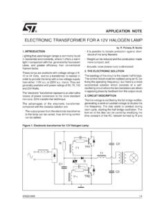
Transcription of An isolated gate drive for Power MOSFETs and IGBTs
1 APPLICATION NOTE. AN isolated GATE drive FOR Power MOSFETs AND IGBTs by Bourgeois ABSTRACT 1. INTRODUCTION. Power MOSFET and IGBT gate drives often isolated Power switches are often used in face isolation and high voltage constraints. motor drives, uninterruptible Power supplies The gate drive described in this paper uses and AC switches. Isolation is usually a a Printed Circuit Board based transformer requirement of safety norms and operating in combination with the memory effect of conditions when the switch voltage floats the Power MOSFET input capacitance to with respect to ground. achieve the isolation. This paper highlights a specific characteristic This transformer is a bi-directional link of the Power MOSFET which is often between the ground-referenced control IC neglected: the use of the gate input and the floating gate drive . It transfers drive capacitance as an ON state memory.
2 It energy and signal information to the gate proposes an innovative isolated gate drive drive , provides full duty cycle range and using a pulse transformer constructed using perfect dV/dt immunity, and imposes virtually copper PCB tracks, combined with the no voltage constraint. No floating auxiliary memory effect of the Power MOSFET. supply is required. If the short circuit protection is triggered, an 2. PRINCIPLES OF OPERATION. alarm signal is transmitted back to the primary through the same transformer. This The circuit operates using the Power circuit is perfectly suited to driving floating MOSFET input capacitance to memorize and/or isolated switches in motor drives, the ON-state, a second auxiliary capacitor uninterruptible Power supplies and AC to memorize the OFF-state, and PCB tracks switches. to form the windings of the transformer. AN461/0194 1/7. APPLICATION NOTE. The transformer is driven by pulses in bi- 3.
3 IMPLEMENTATION. directional mode; when a voltage pulse is The circuit shown in figure 1 implements applied across the primary, energy is these principles. The Power MOSFET or transmitted to the secondary and the state IGBT input capacitance memorizes its ON- of the Power MOSFET is defined (ON or state. The capacitor C7 memorizes the OFF- OFF). After the primary pulse, in the steady state and maintains a low impedance state, an alarm signal can be transmitted between the gate and source terminals from the secondary to the primary if a short during the OFF-state via T7. Short circuit circuit is detected. Figure 1: Circuit implementing isolated gate drive protection with masking of the free wheeling refresh of the memory capacitances. diode recovery current is implemented with The circuit shown in figure 5 is a simplified T6, T8 and T9. If the circuit is to be operated version of that shown in figure 1.
4 Under 1kHz, provision must be made for 2/7. APPLICATION NOTE. 4. FUNCTIONAL DESCRIPTION Primary circuit Figure 2 shows a block diagram of the circuit. The TD300 is a three channel MOSFET. It consists of a TD300 pulse transformer driver with pulse transformer driving driver, a PCB based transformer and an capability. It has been optimized for both isolated secondary circuit. capacitive load drive and pulse transformer demagnetization. Figure 2: Circuit block diagram It can therefore directly drive a low side Pulse transformer switch and, through a pulse transformer, an The pulse width required to fully charge the high side switch. Its low buffer RDS(ON) can gate capacitance is typically around 1 sec. conduct a demagnetizing current of 100mA. Supposing that double pulses can occur with no significant voltage drop. The during the operation, the maximum transformer inductance can therefore be kept product is 30V/ sec.
5 With a low, and the transformer windings can be magnetizing current of 100mA, the primary implemented with few turns laid on a Printed transformer inductance required is: Circuit Board. L = V . (di/dt)-1 = 300 H. The TD300 integrates three additional circuits enabling protection and control This low value of inductance allows the functions: an undervoltage lockout, an primary winding to be limited to 10 turns operational amplifier and a comparator. using a realistic section of ferrite. 3/7. APPLICATION NOTE. Figure 3 shows an implementation using Experimental tests showed that the PCB tracks to form the inductor. Track widths magnetizing current reaches 100mA after are 12 mils at the primary and 10 mils at the 2 sec using a standard A4-U-1606A made secondary. The inter-line distance is 4 mils of high permeability material ( i = 6000 - in both cases (mask definition). standard THOMSON Passive Components).
6 Figure 3: PCB layout: a) Upper side b) Lower side a) b). However the magnetic path of this U core is pulse transformer primary. When the primary too long for through-hole applications. Using pulse ends, the transformer secondary a bus bar core shape with the same section voltage is approximately zero, and the diode but with shorter legs to fit the PCB, the D prevents Cin from being discharged. magnetizing current should fall to 60mA. It In figure 4b, the MOSFET keeps its gate is then possible to increase the pulse time charge after the pulse and remains in the or to decrease the core section to obtain a conducting state. The ON-state is magnetizing current of 100mA. memorized in the input capacitor Cin. Secondary circuit Turn-OFF pulse: Figure 4c shows the input Many different secondary circuit topologies capacitor discharge current I d when a can be used, depending on application negative pulse is applied across the pulse performance and cost.
7 The cheapest solution transformer primary. Discharge occurs when uses one zener diode and one resistor, but an additional circuit transfers the secondary the digital control is more complex, and it voltage to the auxiliary capacitor Caux, making has no floating short circuit protection (see Taux conduct. When the pulse ends, the OFF- reference 6). state is memorized in the auxiliary capacitor. A low impedance is then maintained across For more sophisticated applications, figure the Power switch, avoiding unwanted turn- 4 shows a step by step analysis of the on (see figure 4d). secondary circuit shown in figure 1. Short circuit protection: A short circuit Turn-ON pulse: figure 4a shows the charge can be detected by means of a shunt or current Ic of the MOSFET input capacitor current sense. Then, the diode D is shorted, when a positive pulse is applied across the 4/7. APPLICATION NOTE.
8 Figure 4: Details of circuit operation a) b). c) d). e) f). allowing the Power input capacitor to Diode recovery current: Generally, inverter discharge through the pulse transformer just Power switches face a diode recovery current after the turn-on pulse. This produces a at turn on. This creates a brief over-current negative current pulse in the transformer in the switch that requires masking from the secondary, enabling the short circuit to be short circuit detection during the recovery detected via the primary winding. Indeed, time. this discharge current inverts the Due to the Miller effect, the current Ic lasts demagnetizing current temporarily, inverting for as long as the collector/drain voltage the buffer output voltage (see current I d, falls. Inhibiting the short circuit detection by figure 4e). The short circuit conduction time means of Ic masks all the diode recovery is approximately the turn-on pulse time.
9 Current (see figure 4f). 5/7. APPLICATION NOTE. 5. MAIN FEATURES OF THE CIRCUIT. No floating auxiliary supply Low energy and cheap transformer The Power MOSFET switches are supplied The energy transferred to the secondary by by pulses from the transformer. No floating the pulse transformer is (on average per auxiliary supply is required. cycle) about four times the energy stored in the gate capacitor (average current of about Large operating frequency range 2mA at 10kHz for 50nF). The transformer This driver can operate at up to several tens magnetizing energy must be added two of kiloHertz because the transformer delivers times per cycle (average current of about very short pulses, typically 500nsec or 1 sec. 2mA at 10kHz for 300 H), so global driver If DC or very low frequency operation is energy consumption is very small. required, circuits to perform an automatic The construction of the transformer can be refresh of memory capacitors must be automated using PCB based windings.
10 Implemented; the primary circuit should then drive the transformer with a burst of positive Good ground to gate drive isolation or negative pulses. (see reference 6). and perfect dV/dt immunity Large duty cycle Because the pulse transformer provides the isolation, creepage distance and clearance Again because of the length of the are easily adjusted to suit the application transformer pulses, the possible range of requirements. duty cycles is large: the minimum ON or OFF time is about 500nsec, allowing the The primary-secondary electrostatic coupling duty cycle to range from 1% to 99% at effects are negligible, and immunity to fast 20kHz. There is no maximum ON or OFF voltage variations (dV/dt) is perfect. time. Figure 5: Simplified circuit 6/7. APPLICATION NOTE. Low gate drive output impedance automation of the transformer construction during OFF-state process. During its OFF-state, a low impedance is Its major fields of application are motor maintained across the gate-source terminals drives, uninterruptible Power supplies and of the Power MOSFET, avoiding unwanted AC switches.
