Transcription of AN920/D Theory and Applications of the MC34063 and …
1 Semiconductor Components Industries, LLC, 2013 December, 2013 Rev. 61 Publication Order Number:AN920/DAN920/DTheory and Applications of the MC34063 andmA78S40 SwitchingRegulator control CircuitsThis paper describes in detail the principle of operation of the MC34063 and A78S40 switching regulator subsystems. Severalconverter design examples and numerous Applications circuits with test data are MC34063 and A78S40 are monolithic switchingregulator subsystems intended for use as dc to dc devices represent a significant advancement in theease of implementing highly efficient and yet simpleswitching power supplies. The use of switching regulatorsis becoming more pronounced over that of linear regulatorsbecause the size reductions in new equipment designsrequire greater conversion efficiency. Another majoradvantage of the switching regulator is that it has increasedapplication flexibility of output voltage.
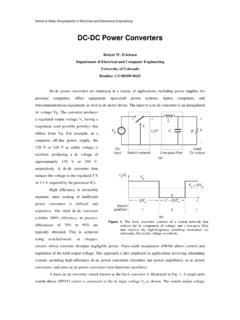
2 The output can beless than, greater than, or of opposite polarity to that of theinput OF OPERATIONIn order to understand the difference in operation betweenlinear and switching regulators we must compare the blockdiagrams of the two step down regulators shown in Figure1. The linear regulator consists of a stable reference, a highgain error amplifier, and a variable resistance series passelement. The error amplifier monitors the output voltagelevel, compares it to the reference and generates a linearcontrol signal that varies between two extremes, saturationand cutoff. This signal is used to vary the resistance of theseries pass element in a corrective fashion in order tomaintain a constant output voltage under varying inputvoltage and output load switching regulator consists of a stable reference anda high gain error amplifier identical to that of the linearregulator. This system differs in that a free running oscillatorand a gated latch have been added.
3 The error amplifier againmonitors the output voltage, compares it to the referencelevel and generates a control signal. If the output voltage isbelow nominal, the control signal will go to a high state andturn on the gate, thus allowing the oscillator clock pulses todrive the series pass element alternately from cutoff tosaturation. This will continue until the output voltage ispumped up slightly above its nominal value. At this time, thecontrol signal will go low and turn off the gate, terminatingany further switching of the series pass element. The outputvoltage will eventually decrease to below nominal due to thepresence of an external load, and will initiate the switchingprocess again. The increase in conversion efficiency isprimarily due to the operation of the series pass elementonly in the saturated or cutoff state. The voltage drop acrossthe element, when saturated, is small as is the in cutoff, the current through the element and likewisethe power dissipation are also small.
4 There are othervariations of switching control . The most common are thefixed frequency pulse width modulator and the fixedon time variable off time types, where the on offswitching is uninterrupted and regulation is achieved byduty cycle control . Generally speaking, the example givenin Figure 1b does apply to MC34063 and 1. Step Down Regulators+ VinVoutRefVoltageErrorAmpLinear ControlSignal+ VinVoutRefVoltageErrorAmpDigitalControl SignalGatedLatchOSCa. Linear Regulatorb. Switching RegulatorAPPLICATION DESCRIPTIONThe MC34063 series is a monolithic control circuitcontaining all the active functions required for dc to dcconverters. This device contains an internal temperaturecompensated reference, comparator, controlled duty cycleoscillator with an active peak current limit circuit, driver,and a high current output switch. This series was specificallydesigned to be incorporated in step up, step down andvoltage inverting converter Applications .
5 These functionsare contained in an 8 pin dual in line package shown inFigure A78S40 is identical to the MC34063 with theaddition of an on board power catch diode, and anuncommitted operational amplifier. This device is in a16 pin dual in line package which allows the reference andthe noninverting input of the comparator to be pinned additional features greatly enhance the flexibility ofthis part and allow the implementation of more sophisticatedapplications. These may include series pass regulation ofthe main output or of a derived second output voltage, atracking regulator configuration or even a second DESCRIPTIONThe oscillator is composed of a current source and sinkwhich charges and discharges the external timing capacitorCT between an upper and lower preset threshold. The typicalcharge and discharge currents are 35 A and 200 Arespectively, yielding about a one to six ratio.
6 Thus theramp up period is six times longer than that of theramp down as shown in Figure 3. The upper threshold isequal to the internal reference voltage of V and thelower is approximately equal to V. The oscillator runscontinuously at a rate controlled by the selected value of the ramp up portion of the cycle , a Logic 1 ispresent at the A input of the AND gate. If the outputvoltage of the switching regulator is below nominal, a Logic 1 will also be present at the B input. This condition willset the latch and cause the Q output to go to a Logic 1 ,enabling the driver and output switch to conduct. When theoscillator reaches its upper threshold, CT will start todischarge and Logic 0 will be present at the A input ofthe AND gate. This logic level is also connected to aninverter whose output presents a Logic 1 to the reset inputof the latch. This condition will cause Q to go low,disabling the driver and output switch.
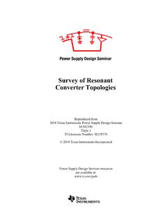
7 A logic truth table ofthese functional blocks is shown in Figure output of the comparator can set the latch only duringthe ramp up of CT and can initiate a partial or full on cycleof output switch conduction. Once the comparator has setthe latch, it cannot reset it. The latch will remain set until CTbegins ramping down. Thus the comparator can initiateoutput switch conduction, but cannot terminate it and thelatch is always reset when CT begins ramping down. Thecomparator s output will be at a Logic 0 when the outputvoltage of the switching regulator is above nominal. Underthese conditions, the comparator s output can inhibit aportion of the output switch on cycle , a complete cycle , acomplete cycle plus a portion of one cycle , multiple cycles,or multiple cycles plus a portion of one 2. Functional Block Diagrams87651234Q1Q2 SRQL atchBASwitchCollectorSwitchEmitterTiming CapacitorGroundDriveCollectorIpkSenseVCC C omparatorInvertingInputIpkCTOSC+ VReferenceRegulatora.
8 MC34063b. mA78S4098107116125134143152161 SwitchCollectorDriverCollectorIpk SenseVCCT imingCapacitorGNDI nvertingInputNoninvertingInputDiodeCatho deDiodeAnodeVCCOp VRefCTIpkOSC+ D1170AB+ SRQL atchOpAmpCompGNDComp170 Figure 3. CT Voltage WaveformVtUpper Threshold V TypicalLower Threshold V TypicaltDischarge6t ChargeAN920/ Condition ofTiming Capacitor, CTAND Gate InputsLatch InputsOutputSwitchComments on State of Output SwitchABSRB egins Ramp Up000 Switching regulator s output is nominal ( B = 0).Begins Ramp Down000No change since B was 0 before CT Ramp Down0010No change even though switching regulator soutput < nominal. Output switch cannot beinitiated during RT Ramp Down0010No change since output switch conductionwas terminated when A went to Up10 Switching regulator s output went < nominalduring CT Ramp Up ( B 1). Partial on cycle for output Up101 Switching regulator s output went nominal( B 0) during CT Ramp Up.
9 No changesince B cannot reset Ramp Up1 Complete on cycle since B was 1 before CTstarted Ramp Ramp Down1 Output switch conduction is always termi-nated whenever CT is Ramping 4. Logic Truth Table of Functional BlocksCurrent limiting is accomplished by monitoring thevoltage drop across an external sense resistor placed in serieswith VCC and the output switch. The voltage drop developedacross this resistor is monitored by the Ipk Sense pin. Whenthis voltage becomes greater than 330 mV, the current limitcircuitry provides an additional current path to charge thetiming capacitor CT. This causes it to rapidly reach the upperoscillator threshold, thereby shortening the time of outputswitch conduction and thus reducing the amount of energystored in the inductor. This can be observed as an increasein the slope of the charging portion of the CT voltagewaveform as shown in Figure 5. Operation of the switchingregulator in an overload or shorted condition will cause avery short but finite time of output conduction followed byeither a normal or extended off time internal provided bythe oscillator ramp down time of CT.
10 The extended intervalis the result of charging CT beyond the upper oscillatorthreshold by overdriving the current limit sense input. Thiscan be caused by operating the switching regulator with aseverely overloaded or shorted output or having the inputvoltage grossly above the nominal design OperationStartupFigure 5. Typical Operating WaveformsComparator OutputTiming Capacitor, CTOutput SwitchNominal Output VoltageLevelOutput VoltageOnOff10AN920/ 6. Timing Capacitor Charge Current versusCurrent Limit Sense Voltage0 Ichg, Charging Current (mA)VCLS, Current Limit Sense Voltage (V) = 25 CVCC = 40 VVCC = 5 VIchg = IdischgUnder extreme conditions, the voltage across CT willapproach VCC and can cause a relatively long off time. Thisaction may be considered a feature since it will reduce thepower dissipation of the output switch considerably. Thisfeature may be disabled on the A78S40 only, by connectinga small signal PNP transistor as a clamp.