Example: bachelor of science
Analog CMOS/VLSI Design - USF College of Engineering
Analog CMOS/VLSI Design (G and UG; also on-line) Analog CMOS/VLSI is the essential ingredient for sensor chips, digital cameras, communication and networking chips, security chips, and very
Tags:
Information
Domain:
Source:
Link to this page:
Documents from same domain

On-Chip Point-of-Load Voltage Regulator for Distributed ...
www.eng.usf.eduAn ultra-low area, current efficient voltage regulator appro- ... On-chip voltage regulator, power delivery, DC-DC voltage regulation, active filter 1. INTRODUCTION ... linear voltage regulator is proposed for distributed point-of-load voltage regulation. This circuit provides a means for

Distributed Power Network Co-Design with On-Chip Power ...
www.eng.usf.eduOn-Chip Power Supplies and Decoupling Capacitors ... complicates the analysis of the power distribution network. Inter-actions among the on-chip power supplies, decoupling capacitors, ... A representative power delivery network with on-chip power supplies, decoupling capacitors, and …
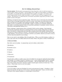
How To: Outlining a Research Paper Note for students: This ...
www.eng.usf.eduword choice, and transitional sentences (etc.). Before continuing, I should mention what you should do before serious outlining. Some important ... replace the general topic headings used above with specific heading phrases that are relevant to your paper's topic. (Some description of the meanings of the headings listed above are provided in
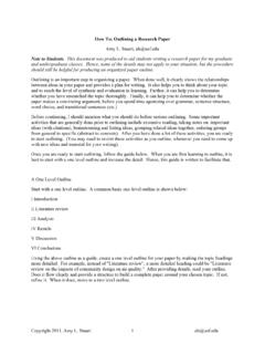
How To: Outlining a Research Paper
www.eng.usf.eduA two level outline is made up of headings for sections and subsections of a paper. A heading is a short phrase that describes the topic area of the section or subsection represented. A basic, two-level outline with many of the common elements in a research paper is shown below: I Introduction A. Motivation (Why this work is important)

Chapter 3 Micromechanical Analysis of a Lamina - USF
www.eng.usf.eduvolume fraction and comparison with experimental values for a unidirectional glass/epoxy lamina (Gf = 30.19 GPa, Gm = 1.83 GPa). Figure (b) zooms figure (a) for fiber volume fraction between 0.45 and 0.75. (Experimental data from Hashin, Z., NASA tech. rep. contract no. NAS1-8818, November 1970.)
Related documents

Lecture 1: Circuits & Layout - cmosvlsi.com
www.cmosvlsi.comCMOS VLSI Design Lecture 1: Circuits & Layout David Harris Harvey Mudd College Spring 2004. 1: Circuits & Layout CMOS VLSI Design Slide 2 Outline qA Brief History qCMOS Gate Design ... Circuits & Layout CMOS VLSI Design Slide 45 Gate Layout qLayout can be very time consuming – Design gates to fit together nicely

Fundamentals of CMOS VLSI 10EC56 - Weebly
vmracetechnology.weebly.comFundamentals of CMOS VLSI 10EC56 CITSTUDENTS.IN Page- 4 3 UNIT 3: CMOS LOGIC STRUCTURES 67-78 CMOS Complementary Logic, 67 Bi CMOS Logic 67-68 Pseudo-nMOS Logic 69-70 Dynam icCMOS Log 71 CMOS D omin Log icC asca de V l tge Sw h g (CVSL).

Lecture 9: Circuit Families - cmosvlsi.com
www.cmosvlsi.comCMOS VLSI Design Lecture 9: Circuit Families David Harris Harvey Mudd College Spring 2004. 9: Circuit Families CMOS VLSI Design Slide 2 Outline qPseudo-nMOS Logic qDynamic Logic ... Circuit Families CMOS VLSI Design Slide 25 Leakage qDynamic node floats high during evaluation – Transistors are leaky (I

Analog CMOS/VLSI Design - USF
ugs.usf.eduUSF: Analog CMOS VLSI Design. Spring 2014 1 Catalog Description: Design of analog circuits for CMOS/VLSI design. Op-amps, comparators, D to A and A to D converters. Switched capacitor filters.

Iddq Testing for CMOS VLSI - cs.colostate.edu
www.cs.colostate.eduIddq Testing for CMOS VLSI Rochit Rajsuman, SENIOR MEMBER, IEEE It is little more than 15-years since the idea of Iddq testing was first proposed. Many semiconductor companies now consider Iddq

Lecture 14: Wires - User page server for CoE
user.engineering.uiowa.edu14: Wires CMOS VLSI Design 4th Ed. 22 Crosstalk Delay Assume layers above and below on average are quiet – Second terminal of capacitor can be ignored – Model as C gnd = C top + C bot Effective C adj depends on behavior of neighbors

CMOS Transistor Theory - pages.hmc.edu
pages.hmc.edu3: CMOS Transistor Theory 3CMOS VLSI DesignCMOS VLSI Design 4th Ed. Introduction So far, we have treated transistors as ideal switches An ON transistor passes a finite amount of current

ECEN474/704: (Analog) VLSI Circuit Design Spring 2018
ece.tamu.eduAgenda • MOS Fabrication Sequence • CMOS Design Rules • Layout Techniques • Layout Examples 3

CMOS VLSI Design - Harvey Mudd College
pages.hmc.eduFourth Edition Neil H. E. Weste Macquarie University and The University of Adelaide David Money Harris Harvey Mudd College CMOS VLSI Design A Circuits and Systems Perspective
CMOS VLSI Design Techniques - University of Southern ...
www-classes.usc.edudesigns&that&are&highly&optimized&but&are&too&late&for&products&that&have&planned& timing.&&& Thefinalchallengeisonethatkeeps theauthorinterestedinteachingwhatappears&
Related search queries
Lecture 1: Circuits & Layout, Cmosvlsi, CMOS VLSI, Fundamentals of CMOS VLSI 10EC56, CMOS, Lecture 9: Circuit Families, Analog CMOS/VLSI Design, Analog CMOS VLSI Design, CMOS/VLSI, Iddq testing, 14: Wires, 14: Wires CMOS VLSI, CMOS Transistor Theory, VLSI, ECEN474/704: (Analog) VLSI Circuit Design, CMOS VLSI Design, CMOS VLSI Design Techniques