Transcription of Analysis of Trace Metals on Wafer Edge and Bevel
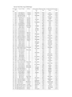
1 Copyright @ ChemTrace March 2018contact us at of Trace Metals on Wafer Edge and Bevel BY AUTOMATED VPD ICP-MSWafer edge exclusion zone is a major source of contamination as it comes in contact with processing equipment. Transition to copper interconnects, low-k dielectrics as well as decreasing gate lengths in semiconductor manufacturing have resulted in bigger yield hits due to presence of Trace metal impurities on Wafer Bevel and edge exclusionTABLE 1. Bevel EDGE Trace METAL METHOD DETECTION LIMITS OR 300mm WAFERSS urface Concentration (x1010 atoms/cm2)ElementOne Sided BevelEntire Bevel Phase Decomposition (VPD) and Inductively Coupled Plasma - Mass Spectrometry (ICP-MS) is the most utilized technique for analyzing Trace metal contamination on Wafer surfaces owing to its superior sensitivity and capability to analyze low to high Z offers this technique for one-sided Bevel or entire Bevel edge Analysis using an Automated VPD ICP-MS with excellent method detection limits (MDL s) and spike recoveries, see Tables 1 and 2.
2 Using this technique, the scanning precision for 2mm scan is controlled to from both front and back of the 2. SPIKE RECOVERY % FROM Bevel EDGE SCANE lementFull BevelOne Side Bevel101%96%55%91%105%81%35%92%102%102%1 01%79%102%84%107%AlSbAsBaBeBiBCdCaCrCoCu GaGeFe104%80%54%76%85%65%39%81%108%85%86 %65%83%70%98%ElementFull BevelOne Side Bevel96%102%115%100%107%112%104%104%98%1 07%115%93%99%103%97%83%87%94%85%88%91%92 %95%85%90%107%80%85%84%79%PbLiMgMnMoNiKN aSrSnTiWVZnZrCopyright @ ChemTrace March 2018contact us at High degree of scanning repeatability Scanning accuracy to Wafer sizes of 200-450mm Excellent Method Detection Limits 40 plus elements in one scan Fully quantitative Good spike recoveries (75-125%) for most elements