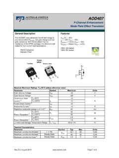
Transcription of AOD4189 P-Channel Enhancement Mode Field Effect Transistor
1 SymbolVDSVGSIDMIAREARTJ, TSTGS ymbolTypMax15204150R to DrainCurrent B,HMaximumUnitsParameterTC=25 CTC=100 C-40 Absolute Maximum Ratings TC=25 C unless otherwise notedVTA=70 CPower Dissipation BAvalanche Current CRepetitive avalanche energy L= CAmJIDP ulsed Drain Current C-40-28-50-3561V 20 Gate-Source VoltageDrain-Source VoltageSteady-StateTA=25 CPDSMTC=25 CMaximum Junction-to-Ambient A,GSteady-StatePower Dissipation AJunction and Storage Temperature RangePDTC=100 C C/WThermal CharacteristicsParameterUnitsMaximum Junction-to-Ambient A,Gt 10sR JA C/W C/WMaximum Junction-to-Case D,FAOD4189P-Channel Enhancement Mode Field Effect TransistorFeaturesVDS (V) = -40 VID = -40A (VGS = -10V)RDS(ON) < 22m (VGS = -10V)RDS(ON) < 29m (VGS = ) 100% UIS Tested! 100% Rg Tested!General DescriptionThe AOD4189 uses advanced trench technology anddesign to provide excellent RDS(ON) with low gatecharge.
2 With the excellent thermal resistance of theDPAK package, this device is well suited for highcurrent load applications. -RoHS Compliant -Halogen Free*GDS GTO-252D-PAKTop View SBottom View D G SAlpha & Omega Semiconductor, Typ Max UnitsBVDSS-40V-1TJ=55 C-5 IGSS 100nAVGS(th) (ON)-50A1822TJ=125 Qg (-10V) ( ) (on)10nstr18nstD(off)38nstf24nstrr3242ns Qrr30nCCOMPONENTS IN LIFE SUPPORT DEVICES OR SYSTEMS ARE NOT AUTHORIZED. AOS DOES NOT ASSUME ANY LIABILITY ARISINGOUT OF SUCH APPLICATIONS OR USES OF ITS PRODUCTS. AOS RESERVES THE RIGHT TO IMPROVE PRODUCT DESIGN,FUNCTIONS AND RELIABILITY WITHOUT Source ChargeGate resistanceVGS=0V, VDS=0V, f=1 MHzVGS=-10V, VDS=-20V,ID=-12 ATBDT otal Gate Chargem Turn-On Rise TimeTurn-Off DelayTimeVGS=-10V, VDS=-20V, RL= ,RGEN=3 Turn-Off Fall TimeTurn-On DelayTimeGate Drain ChargeVGS=0V, VDS=-20V, f=1 MHzSWITCHING PARAMETERST otal Gate ChargeVGS= , ID=-8 AIS=-1A,VGS=0 VVDS=-5V, ID=-12 AMaximum Body-Diode Continuous CurrentInput CapacitanceOutput CapacitanceDYNAMIC PARAMETERSRDS(ON)Static Drain-Source On-ResistanceForward TransconductanceDiode Forward VoltageElectrical Characteristics (TJ=25 C unless otherwise noted)
3 STATIC PARAMETERSP arameterConditionsIDSS ABody Diode Reverse Recovery ChargeIF=-12A, dI/dt=100A/ sBody Diode Reverse Recovery TimeVGS=-10V, ID=-12 AReverse Transfer CapacitanceIF=-12A, dI/dt=100A/ sGate Threshold VoltageVDS=VGS ID=-250 ADrain-Source Breakdown VoltageOn state drain currentID=-250 A, VGS=0 VVGS=-10V, VDS=-5 VVDS=-40V, VGS=0 VVDS=0V, VGS= 20 VZero Gate Voltage Drain CurrentGate-Body leakage currentA: The value of R JA is measured with the device in a still air environment with TA =25 C. The power dissipation PDSM and current rating IDSM arebased on TJ(MAX)=150 C, using steady state junction-to-ambient thermal The power dissipation PD is based on TJ(MAX)=175 C, using junction-to-case thermal resistance, and is more useful in setting the upperdissipation limit for cases where additional heatsinking is : Repetitive rating, pulse width limited by junction temperature TJ(MAX)=175 The R JA is the sum of the thermal impedence from junction to case R JC and case to The static characteristics in Figures 1 to 6 are obtained using t 300 s pulses, duty cycle These curves are based on the junction-to-case thermal impedence which is measured with the device mounted to a large heatsink, assuminga maximum junction temperature of TJ(MAX)=175 C.
4 The SOA curve provides a single pulse These tests are performed with the device mounted on 1 in2 FR-4 board with 2oz. Copper, in a still air environment with TA=25 The maximum current rating is limited by bond-wires.*This device is guaranteed green after data code 8X11 (Sep 1ST 2008).Rev1: Oct 2008 Alpha & Omega Semiconductor, ELECTRICAL AND THERMAL CHARACTERISTICS150mJ01020304050012345-VD S (Volts)Figure 1: On-Region Characteristics-ID (A)VGS= (Volts)Figure 2: Transfer Characteristics-ID(A)1618202224262830010 203040-ID (A)Figure 3: On-Resistance vs. Drain Current andGate VoltageRDS(ON) (m ) (Volts)Figure 6: Body-Diode Characteristics-IS (A)25 C125 -25 0 25 50 75 100 125 150 175 200 Temperature ( C)Figure 4: On-Resistance vs. JunctionTemperatureNormalized On-ResistanceVGS=-10 VID=-12 AVGS= (Volts)Figure 5: On-Resistance vs. Gate-Source VoltageRDS(ON) (m )VDS=-5 VVGS= C125 C25 C125 CAlpha & Omega Semiconductor, ELECTRICAL AND THERMAL CHARACTERISTICS150mJ02468100510152025303 5Qg (nC)Figure 7: Gate-Charge Characteristics-VGS (Volts)0400800120016002000240028000510 15 20 25 30 35 40-VDS (Volts)Figure 8: Capacitance CharacteristicsCapacitance (pF) Width (s)Figure 10: Single Pulse Power Rating Junction-to-Case (Note F)Power (W) Width (s)Figure 11: Normalized Maximum Transient Thermal Impedance (Note F)Z Jc Normalized TransientThermal ResistanceCossCrss110100110100-VDS (Volts)-ID (Amps)Figure 9.
5 Maximum Forward BiasedSafe Operating Area (Note F)10ms1msDCRDS(ON)limitedTJ(Max)=175 CTC=25 C10 s100 sVDS=-20 VID=-12 ASingle PulseD=Ton/TTJ,PK=Tc+ JCR JC= C/WTonTPDIn descending orderD= , , , , , , single pulseTJ(Max)=175 CTC=25 CAlpha & Omega Semiconductor, ELECTRICAL AND THERMAL CHARACTERISTICS010203040500255075100 125 150 175 TCASE ( C)Figure 14: Current De-rating (Note B)Current rating -ID (A)1101001000100001E-04 100 1000 Pulse Width (s)Figure 15: Single Pulse Power Rating Junction-to-Ambient (Note G)Power (W)TJ(Max)=150 CTA=25 Width (s)Figure 16: Normalized Maximum Transient Thermal Impedance (Note G)Z JA Normalized TransientThermal ResistanceD=Ton/TTJ,PK=TA+ JAR JA=50 C/WSingle PulseTonTPDIn descending orderD= , , , , , , single pulse0102030405060700255075100125150175 TCASE ( C)Figure 13: Power De-rating (Note B)Power Dissipation (W) in Avalache, tA (s)Figure 12: Single Pulse Avalanche Capability-IA, Peak Avalanche Current (A)Alpha & Omega Semiconductor, Charge Test Circuit & Waveform-+-+-10 VVddVgsIdVgsRgDUTVDCVgsVdsIdVgsUnclamped Inductive Switching (UIS) Test Circuit & WaveformsVdsL-+2E = 1/2 LIARARBVDSSIARIgVgs-+VDCDUTLVgsIsdDiode Recovery Test Circuit & WaveformsVds -Vds +dI/dtRMrrVddVddQ = - Idttrr-Isd-VdsF-I-IVDCDUTVddVgsVdsVgsRLR gResistive Switching Test Circuit & Waveforms-+VgsVdstttttt90%10%rond(off)fo ffd(on)Alpha & Omega Semiconductor.