Transcription of Application Notes - OSI Optoelectronics
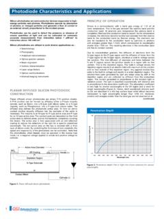
1 74 Figure Optoelectronics , is a leading manufacturer of fiber optic components for communication systems. The products offer range for Silicon, GaAs and InGaAs to full turnkey are semiconductor devices responsive to high energy particles and photons. Photodiodes operate by absorption of photons or charged particles and generate a flow of current in an external circuit, proportional to the incident power. Planar diffused silicon photodiodes are P-N junction diodes. A P-N junction can be formed by diffusing either a P-type impurity, such as Boron, into a N-type bulk or epitaxial silicon wafer, or a N-type impurity, such as Phosphorus, into a P-type bulk or epitaxial wafer. The diffused area defines the photodiode active area. To form an ohmic contact, another impurity diffusion into the backside of the wafer is necessary.
2 The active area is coated with an Anti-Reflection coating to reduce the reflection of the light for a specific predefined wavelength. The P and N-sides of the junction have metal pads, which make an electrical contact through dielectric applications within the wavelength range of m - m, photodiodes made on InGaAs/InP material are widely used due to the superior speed, responsivity and low noise characteristics. Figure shows the schematic cross-section of OSI Optoelectronics s InGaAs/InP to the high absorption coefficient, the InGaAs absorption region is typically a few micrometers thick. The thin absorption layer enables the device to obtain high speed at a low reverse bias voltage, typically 2-5 volts. The InP window layer is transparent to m - m wavelengths, thus InGaAs/InP photodiodes do not have slow tail impulse response associated with the slow diffusion component from the contact typical spectral response curves of Silicon, GaAs, and InGaAs photodiodes are shown in Figures , , The bandgap energies of Si, GaAs, and InGaAs are , , and respectively.
3 The cutoff wavelengths of photodiodes made from these materials are m for Si, m for GaAs, and m for InGaAsOSI Optoelectronics s InGaAs/InP photodiodes are planar passivated. The dark current is low and very stable. shows the typical dark current of FCI-InGaAs-500 as a function of reverse bias voltage. The relationship between dark current and temperature is shown in Figure +LAYERN TYPE InGaAs ABSORPTION LAYERN TYPE InP BUFFER LAYERN+ TYPE InP SUBSTRATEMETALLIZATIONInP CAP LAYERAR 500 600 700 800 900 1000 1100 Wavelength (nm)Responsivity (A/W)Typical Spectral Responsivity (Si) 600 800 1000 1080 Wavelength (nm)Responsivity (A/W)Typical Spectral Responsivity (GaAs) 900 1000 1100 1200 1300 1400 1500 1600 1700 1800 Wavelength (nm)Responsivity (A/W)Typical Spectral Responsivity (InGaAs) 0 1 2 3 4 5 6 7 8 9 10 Reverse Bias Voltage (V)Dark Current (A)Typical Dark Current vs.
4 Reverse Bias Voltage (500m InGaAs in TO-package)Figure Notes75 Application NotesElectrical CharacteristicsA p-n junction photodiode can be represented by a current source in parallel with an ideal diode (Figure ). The current source represents the current generated by the incident photons, and the diode represents the p-n junction. In addition, a junction capacitance Cj and a shunt resistance Rsh are in parallel with the other components. Series resistance Rs is connected in series with all components in this Resistance, R shShunt resistance is the slope of the current-voltage curve of the photodiode at the origin, V=0. Although an ideal photodiode should have a shunt resistance of infinite, actual values range from 10s to 1000s of Mega ohms. Experimentally it is usually obtained by applying 10mV, measuring the current and calculating the resistance.
5 Shunt resistance is used to determine the noise current in the photodiode with no bias (photovoltaic mode). For best photodiode performance the highest shunt resistance is Resistance, R sSeries resistance of a photodiode arises from the resistance of the contacts and the resistance of the undepleted semiconductors. It is given by:Where Ws is the thickness of the substrate, Wd is the width of the depleted region, A is the diffused area of the junction, is the resistivity of the substrate and Rc is the contact resistance. Series resistance is used to determine the rise time and the linearity of the Capacitance, C jThe boundaries of the depletion region act as the plates of a parallel plate capacitor. The junction capacitance is directly proportional to the diffused area and inversely proportional to the width of the depletion region.
6 The capacitance is dependent on the reverse bias as follows: Where 0 is the permittivity of free space, is the semiconductor dielectric constant, is the mobility of the majority carriers, is the resistivity, Vbi is the built-in voltage of the semiconductor of the P-N junction and VA is the applied bias. Figure shows the typical capacitance of FCI-InGaAs-500 as a function of the applied reverse bias voltage. Junction capacitance is used to determine the speed of the response of the time and Frequency Response,t r / t f / f 3dBThe rise time and fall time of a photodiode is defined as the time for the signal to rise or fall from 10% to 90% or 90% to 10% of the final value respectively. This parameter can be also expressed as frequency response, which is the frequency at which the photodiode output decreased by 3dB.
7 It is roughly approximated by:+ Figure E-011 0 1 2 3 4 5 6 7 8 9 10 Reverse Bias Voltage (V)Capacitance (F)Typical Capacitance vs. Reverse Bias Voltage (at f=1 MHz, 500m InGaAs in TO-package) 25 35 45 55 65 75 Temperature (C)Dark Current (A)Typical Dark Current vs. Temperature (V=-5V, 500m InGaAs in TO-package)Figure NotesThese are three factors defining the response time of a photodiode: 1. tDRIFT, the drifting time of the carriers in the depleted region of the photodiode. 2. tDIFFUSED, the charge collection time of the carriers in the undepleted region of the photodiode. 3. tRC, the RC time constant of the diode-circuit is determined by tRC= , where R is the sum of the diode series resistance and the load resistance (Rs+RL), and C is the sum of the photodiode junction and the stray capacitances (Cj+Cs). Since the junction capacitance (Cj) is dependent on the diffused area of the photodiode and the applied reverse bias, faster rise times are obtained with smaller diffused area photodiodes, and larger applied biases.
8 In addition, stray capacitance can be minimized by using short leads, and careful lay-out of the electronic components. The total rise time is determined by:NoiseIn a photodiode two sources of noise can be identified. Shot noise and Johnson noise:Shot NoiseShot noise is related to the statistical fluctuation in both the photocurrent and the dark current. The magnitude of the shot noise is expressed as the root mean square (rms) noise current:Where q= is the electron charge, Ip is the photogenerated current, Id is the photodetector dark current and f is the noise measurement or Johnson NoiseThe shunt resistance in the photodetector has a Johnson noise associated with it. This is due to the thermal generation of carriers. The magnitude of the generated current noise is:Where kB= K, is the Boltzmann Constant, T is the absolute temperature in degrees Kelvin (273 K=0 C), f is the noise measurement bandwidth, and Rsh is the shunt resistance of the photodiode.
9 This type of noise is the dominant current noise in photovoltaic (unbias) operation : All resistors have a Johnson noise associated with them, including the load resistor. This additional noise current is large and adds to the Johnson noise current caused by the photodetector shunt NoiseThe total noise current generated in a photodetector is determined by:Noise Equivalent Power(NEP)Noise Equivalent Power is the amount of incident light power on a photodetector, which generates a photocurrent equal to the noise current. NEP is defined as:Where R is the responsivity in A/W and Itn is the total noise of the photodetector. For InGaAs photodiodes, NEP values can vary from10-14W/ Hz for large active area down to 10-15W/ Hz for small active area EFFECTSAll photodiode characteristics are affected by changes in temperature.
10 They include shunt resistance, dark current, breakdown voltage, and to a lesser extent other parameters such as junction Resistance and Dark Current:There are two major currents in a photodiode contributing to dark current and shunt resistance. Diffusion current is the dominating factor in a photovoltaic (unbiased) mode of operation, which determines the shunt resistance. It varies as the square of the temperature. In photoconductive mode (reverse biased), however, the drift current becomes the dominant current (dark current) and varies directly with temperature. Thus, change in temperature affects the photodetector more in photovoltaic mode than in photoconductive mode of photoconductive mode the dark current may approximately double for every 10 C increase change in temperature. And in photovoltaic mode, shunt resistance may approximately double for every 6 C decrease in temperature.