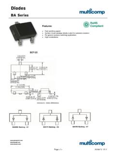
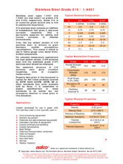
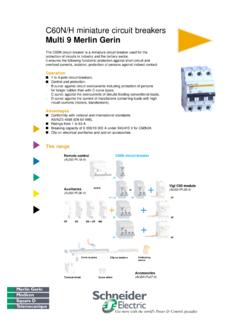
Transcription of BC846, BC847, BC848 Series General Purpose …
1 Semiconductor Components Industries, LLC, 2007 April, 2007 Rev. 51 Publication Order Number: bc846 AWT1/DBC846, BC847, BC848 SeriesGeneral PurposeTransistorsNPN SiliconThese transistors are designed for General Purpose amplifierapplications. They are housed in the SC 70/SOT 323 which isdesigned for low power surface mount Pb Free Packages are AvailableMAXIMUM RATINGSR atingSymbolValueUnitCollector-Emitter VoltageBC846BC847BC848 VCEO654530 VCollector-Base VoltageBC846BC847BC848 VCBO805030 VEmitter-Base Current ContinuousIC100mAdcStresses exceeding Maximum Ratings may damage the device.
2 MaximumRatings are stress ratings only. Functional operation above the RecommendedOperating Conditions is not implied. Extended exposure to stresses above theRecommended Operating Conditions may affect device CHARACTERISTICSC haracteristicSymbolMaxUnitTotal Device Dissipation FR 5 Board,(Note 1) TA = 25 CPD150mWThermal Resistance,Junction to AmbientRqJA833 C/WJunction and Storage TemperatureTJ, Tstg 55 to+150 C1. FR 5 = x x 70/SOT 323 CASE 419 STYLE 3 MARKING DIAGRAMXX= Specific Device CodeM= Month CodeG= Pb Free Package(Note: Microdot may be in either location)XX MGGCOLLECTOR31 BASE2 EMITTER123 See detailed ordering and shipping information in the packagedimensions section on page 5 of this data INFORMATIONBC846, BC847, BC848 CHARACTERISTICS (TA = 25 C unless otherwise noted)CharacteristicSymbolMinTypMaxUnitO FF CHARACTERISTICSC ollector Emitter Breakdown VoltageBC846 Series (IC = 10 mA)BC847 SeriesBC848 SeriesV(BR)CEO654530 VCollector Emitter Breakdown VoltageBC846 Series (IC = 10 mA, VEB = 0)BC847 SeriesBC848 SeriesV(BR)
3 CES805030 VCollector Base Breakdown VoltageBC846 Series (IC = 10 mA)BC847 SeriesBC848 SeriesV(BR)CBO805030 VEmitter Base Breakdown VoltageBC846 Series (IE = mA)BC847 SeriesBC848 SeriesV(BR) VCollector Cutoff Current (VCB = 30 V)(VCB = 30 V, TA = 150 C)ICBO CHARACTERISTICSDC Current GainBC846A, BC847A, BC848A(IC = 10 mA, VCE = V)BC846B, BC847B, BC848 BBC847C, BC848C(IC = mA, VCE = V)BC846A, BC847A, BC848 ABC846B, BC847B, BC848 BBC847C, BC848 ChFE 11020042090150270180290520 220450800 Collector Emitter Saturation Voltage (IC = 10 mA, IB = mA)Base Emitter Saturation Voltage (IC = 100 mA, IB = mA)VCE(sat) Emitter Saturation Voltage (IC = 10 mA, IB = mA)Base Emitter Saturation Voltage (IC = 100 mA, IB = mA)VBE(sat) VBase Emitter Voltage (IC = mA, VCE = V)Base Emitter Voltage (IC = 10 mA, VCE = V)VBE(on)
4 580 660 700770mVSMALL SIGNAL CHARACTERISTICSC urrent Gain Bandwidth Product(IC = 10 mA, VCE = Vdc, f = 100 MHz)fT100 MHzOutput Capacitance (VCB = 10 V, f = MHz)Cobo Figure (IC = mA, VCE = Vdc, RS = kW, f = kHz, BW = 200 Hz)NF 10dBBC846, BC847, BC848 Series & BC848 SERIESF igure 1. Normalized DC Current GainIC, COLLECTOR CURRENT (mAdc) 2. Saturation and On VoltagesIC, COLLECTOR CURRENT (mAdc) 3. Collector Saturation RegionIB, BASE CURRENT (mA)Figure 4. Base Emitter Temperature CoefficientIC, COLLECTOR CURRENT (mA) , NORMALIZED DC CURRENT GAINV, VOLTAGE (VOLTS)VCE, COLLECTOR EMITTER VOLTAGE (V)VB, TEMPERATURE COEFFICIENT (mV/ C) = 25 CVBE(sat) @ IC/IB = 10 VCE(sat) @ IC/IB = 10 VBE(on) @ VCE = 10 VVCE = 10 VTA = 25 C 55 C to +125 CTA = 25 CIC = 50 mAIC = 100 mAIC = 200 mAIC =20 mAIC =10 5.
5 CapacitancesVR, REVERSE VOLTAGE (VOLTS)10 Figure 6. Current Gain Bandwidth ProductIC, COLLECTOR CURRENT (mAdc) = 10 VTA = 25 CC, CAPACITANCE (pF)f , CURRENT GAIN BANDWIDTH PRODUCT (MHz) = 25 CCobCibBC846, BC847, BC848 SERIESF igure 7. DC Current GainIC, COLLECTOR CURRENT (mA)Figure 8. On VoltageIC, COLLECTOR CURRENT (mA) = 25 CVBE(sat) @ IC/IB = 10 VCE(sat) @ IC/IB = 10 VBE @ VCE = VFigure 9. Collector Saturation RegionIB, BASE CURRENT (mA)Figure 10. Base Emitter Temperature CoefficientIC, COLLECTOR CURRENT (mA) , COLLECTOR EMITTER VOLTAGE (VOLTS)VB, TEMPERATURE COEFFICIENT (mV/ C) = 25 C200 mA50 mAIC =10 mAhFE, DC CURRENT GAIN (NORMALIZED)V, VOLTAGE (VOLTS)VCE = 5 VTA = 25 mA20 mA 55 C to 125 CqVB for VBEF igure 11.
6 CapacitanceVR, REVERSE VOLTAGE (VOLTS)40 Figure 12. Current Gain Bandwidth ProductIC, COLLECTOR CURRENT (mA) = 5 VTA = 25 CC, CAPACITANCE (pF)f , CURRENT GAIN BANDWIDTH = 25 CCobCibBC846, BC847, BC848 ORDERING AND SPECIFIC MARKING INFORMATIOND eviceSpecific Marking CodePackageShipping bc846 AWT11 ASC 70 (SOT 323)3,000 / Tape & ReelBC846 AWT1G1 ASC 70 (SOT 323)(Pb Free) bc846 BWT11 BSC 70 (SOT 323)3,000 / Tape & ReelBC846 BWT1G1 BSC 70 (SOT 323)(Pb Free)3,000 / Tape & ReelBC847 AWT11 ESC 70 (SOT 323)3,000 / Tape & ReelBC847 AWT1G1 ESC 70 (SOT 323)(Pb Free)
7 3,000 / Tape & ReelBC847 BWT11 FSC 70 (SOT 323)3,000 / Tape & ReelBC847 BWT1G1 FSC 70 (SOT 323)(Pb Free)BC847 CWT11 GSC 70 (SOT 323)3,000 / Tape & ReelBC847 CWT1G1 GSC 70 (SOT 323)(Pb Free)BC847 CWT3G1 GSC 70 (SOT 323)(Pb Free)10,000 / Tape & ReelBC848 AWT11 JSC 70 (SOT 323)3,000 / Tape & ReelBC848 AWT1G1 JSC 70 (SOT 323)(Pb Free)3,000 / Tape & ReelBC848 BWT11 KSC 70 (SOT 323)3,000 / Tape & ReelBC848 BWT1G1 KSC 70 (SOT 323)(Pb Free) BC848 CWT11 LSC 70 (SOT 323)3,000 / Tape & ReelBC848 CWT1G1 LSC 70 (SOT 323)(Pb Free)3,000 / Tape & Reel For information on tape and reel specifications, including part orientation and tape sizes, please refer to our Tape and Reel Packaging Specifi-cations Brochure, BRD8011 , BC847, BC848 DIMENSIONSSC 70 (SOT 323)CASE 419 04 ISSUE M*For additional information on our Pb Free strategy and solderingdetails, please download the ON Semiconductor Soldering andMounting Techniques Reference Manual, FOOTPRINT*STYLE 3:PIN 1.
8 BASE2. EMITTER3. mminches SCALE 10:1AA2De1beEA1cL312 NOTES:1. DIMENSIONING AND TOLERANCING PER , CONTROLLING DIMENSION: ( ) REFON Semiconductor and are registered trademarks of Semiconductor Components Industries, LLC (SCILLC). SCILLC reserves the right to make changes without further noticeto any products herein. SCILLC makes no warranty, representation or guarantee regarding the suitability of its products for any particular Purpose , nor does SCILLC assume any liabilityarising out of the application or use of any product or circuit, and specifically disclaims any and all liability, including without limitation special, consequential or incidental damages.
9 Typical parameters which may be provided in SCILLC data sheets and/or specifications can and do vary in different applications and actual performance may vary over time. Alloperating parameters, including Typicals must be validated for each customer application by customer s technical experts. SCILLC does not convey any license under its patent rightsnor the rights of others. SCILLC products are not designed, intended, or authorized for use as components in systems intended for surgical implant into the body, or other applicationsintended to support or sustain life, or for any other application in which the failure of the SCILLC product could create a situation where personal injury or death may occur.
10 ShouldBuyer purchase or use SCILLC products for any such unintended or unauthorized application, Buyer shall indemnify and hold SCILLC and its officers, employees, subsidiaries, affiliates,and distributors harmless against all claims, costs, damages, and expenses, and reasonable attorney fees arising out of, directly or indirectly, any claim of personal injury or deathassociated with such unintended or unauthorized use, even if such claim alleges that SCILLC was negligent regarding the design or manufacture of the part. SCILLC is an EqualOpportunity/Affirmative Action Employer.