Transcription of BSS138 - N-Channel Logic Level Enhancement Mode Field ...
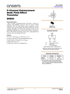
1 DATA Semiconductor Components Industries, LLC, 2005 November, 2021 Rev. 61 Publication Order Number: BSS138 /DN-Channel Logic LevelEnhancement Mode FieldEffect TransistorBSS138 General DescriptionThese N Channel Enhancement mode Field effect transistors areproduced using onsemi s proprietary, high cell density, DMOS technology. These products have been designed to minimize on stateresistance while provide rugged, reliable, and fast switchingperformance. These products are particularly suited for low voltage,low current applications such as small servo motor control, powerMOSFET gate drivers, and other switching A, 50 V RDS(on) = @ VGS = 10 V RDS(on) = @ VGS = V High Density Cell Design for Extremely Low RDS(on) Rugged and Reliable Compact Industry Standard SOT 23 Surface Mount Package This Device is Pb Free and Halogen FreeMARKING DIAGRAMD evicePackageShipping ORDERING INFORMATIONBSS138, BSS138 GSOT 23 3(Pb Free)
2 3000 / Tape & Reel For information on tape and reel specifications,including part orientation and tape sizes, pleaserefer to our Tape and Reel Packaging SpecificationBrochure, BRD8011 23 3 CASE 318 08 SDGSS= Specific Device CodeM= Date Code*G= Pb Free Package(Note: Microdot may be in either location)*Date Code orientation and/or position may varydepending upon manufacturing MAXIMUM RATINGS TA = 25 C unless otherwise Source Voltage50 VVGSSGate Source Voltage 20 IDDrain Current Continuous (Note 1) Current Pulsed (Note 1) Power Dissipation (Note 1) Above 25 CTJ, TSTGO perating and Storage junction Temperature Range 55 to +150 CTLM aximum Lead Temperature for Soldering Purposes, 1/16 from Case for 10 s300 Stresses exceeding those listed in the Maximum Ratings table may damage the device.
3 If any of these limits are exceeded, device functionalityshould not be assumed, damage may occur and reliability may be CHARACTERISTICS TA = 25 C unless otherwise JAThermal Resistance, junction to Ambient (Note 1)350 C/WELECTRICAL CHARACTERISTICS TA = 25 C unless otherwise noted. SymbolParameterTest ConditionsMinTypMaxUnitOFF CHARACTERISTICSBVDSSD rain Source Breakdown VoltageVGS = 0 V, ID = 250 A50 V VGS(th) TJBreakdown Voltage TemperatureCoefficientID = 250 A, Referenced to25 C 72 mV/ CIDSSZero Gate Voltage Drain CurrentVDS = 50 V, VGS = 0 V AVDS = 50 V, VGS = 0 V,TJ = 125 C 5 VDS = 30 V, VGS = 0 V 100nAIGSSGate Body LeakageVGS = 20 V, VDS = 0 V 100ON CHARACTERISTICSVGS(th)Gate Threshold VoltageVDS = VGS, ID = 1 VGS(th) TJGate Threshold Voltage Temperature CoefficientID = 1 mA, Referenced to 25 C 2 mV/ CRDS(on)
4 Static Drain Source On ResistanceVGS = 10 V, ID = A VGS = V, ID = A VGS = 10 V, ID = A,TJ = 125 C (on)On State Drain CurrentVGS = 10 V, VDS = 5 AgFSForward TransconductanceVDS = 10 V, ID = SDYNAMIC CHARACTERISTICSCissInput CapacitanceVDS = 25 V, VGS = 0 V,f = MHz 27 pFCossOutput Capacitance 13 pFCrssReverse Transfer Capacitance 6 pFRGGate ResistanceVGS = 15 mV, f = MHz 9 CHARACTERISTICS TA = 25 C unless otherwise noted. (continued)SymbolUnitMaxTypMinTest ConditionsParameterSWITCHING CHARACTERISTICStd(on)Turn On Delay TimeVDD = 30 V, ID = A,VGS = 10 V, RGEN = 6 On Rise Time 918nstd(off)Turn Off Delay Time 2036nstfTurn Off Fall Time 714nsQgTotal Gate ChargeVDS = 25 V, ID = A,VGS = 10 V Source Charge nCQgdGate Drain Charge nCDRAIN SOURCE DIODE CHARACTERISTICS AND MAXIMUM RATINGSISM aximum Continuous Drain Source Diode Forward Current Source Diode Forward VoltageVGS = 0 V, IS = A (Note 2)
5 Parametric performance is indicated in the Electrical Characteristics for the listed test conditions, unless otherwise noted. Productperformance may not be indicated by the Electrical Characteristics if operated under different R JA is the sum of the junction to case and case to ambient thermal resistance where the case thermal reference is defined as the soldermounting surface of the drain pins. R JA is guaranteed by design while R JA is determined by the user s board ) 350 C/W when mounted on a minimum Pulse Test: Pulse Width 300 s, Duty Cycle CHARACTERISTICSF igure 1.
6 On Region CharacteristicsFigure 2. On Resistance Variation with DrainCurrent and Gate , Drain Current (A)RDS(on), Normalized Drain Source On ResistanceVDS, Drain To Source Voltage (V)ID, Drain Current (A)VGS = 10 V9 = V10 CHARACTERISTICS (continued)Figure 3. On Resistance Variation with TemperatureFigure 4. On Resistance Variation withGate to Source Voltage 50 , Gate To Source Voltage (V)RDS(on), On Resistance (W)TJ, junction Temperature (5C)RDS(on), Normalized Drain Source On = 220 mAVGS = 10 VTA = 25 CTA = 125 CID = 110 5. Transfer CharacteristicsFigure 6.
7 Body Diode Forward Voltage Variationwith Source Current and , Body Diode Forward Voltage (V)IS, Reverse Drain Current (A)VGS, Gate To Source Voltage (V)ID, Drain Current (A) = 55 C25 C125 CVDS = 10 VTA = 125 C25 C 55 CVGS = 0 V1 Figure 7. Gate Charge , Drain To Source Voltage (V)Capacitance (pF)Qg, Gate Charge (nC)VGS, Gate Source Voltage (V)68100204060100010 20 = 220 mA30 V25 VVDS = 8 V80 CISSCOSSCRSSF igure 8. Capacitance 9. Maximum Safe Operating AreaFigure 10. Single Pulse Maximum Power , Time (s)P(pk), Peak Transient Power (W)VDS, Drain Source Voltage (V)ID, Drain Current (A) (on) LimitVGS = 10 VSingle PulseR JA = 350 C/WTA = 25 CDC1 s100 ms10 ms1 ms100 sSingle PulseR JA = 350 C/WTA = 25 C1000 Figure 11.
8 Transient Thermal Response , Time (s)r(t), Normalized Effective TransientThermal = JA(t)= r(t) * R JAR JA = 350 C/WTJ TA = P * R JA(t)Duty Cycle, D = t1 / t2t1t2P(pk)110100 Thermal characterization performed using the conditions described in Note thermal response will change depending on the circuit board 23 (TO 236)CASE 318 08 ISSUE ASDATE 30 JAN 2018 SCALE 4:1DA13121 XXXMGGXXX = Specific Device CodeM= Date CodeG= Pb Free Package*This information is generic. Please refer todevice data sheet for actual part Free indicator, G or microdot G ,may or may not be DIAGRAM*NOTES:1.
9 DIMENSIONING AND TOLERANCING PER ASME , CONTROLLING DIMENSION: MAXIMUM LEAD THICKNESS INCLUDES LEAD LEAD THICKNESS IS THE MINIMUM THICKNESS OFTHE BASE DIMENSIONS D AND E DO NOT INCLUDE MOLD FLASH,PROTRUSIONS, OR GATE FOOTPRINTVIEW VIEW 22:PIN 1. RETURN2. OUTPUT3. INPUTSTYLE 6:PIN 1. BASE2. EMITTER3. COLLECTORSTYLE 7:PIN 1. EMITTER2. BASE3. COLLECTORSTYLE 8:PIN 1. ANODE2. NO CONNECTION3. CATHODESTYLE 9:PIN 1. ANODE2. ANODE3. CATHODESTYLE 10:PIN 1. DRAIN2. SOURCE3. GATESTYLE 11:PIN 1. ANODE2. CATHODE3. CATHODE ANODESTYLE 12:PIN 1.
10 CATHODE2. CATHODE3. ANODESTYLE 13:PIN 1. SOURCE2. DRAIN3. GATESTYLE 14:PIN 1. CATHODE2. GATE3. ANODESTYLE 15:PIN 1. GATE2. CATHODE3. ANODESTYLE 16:PIN 1. ANODE2. CATHODE3. CATHODESTYLE 17:PIN 1. NO CONNECTION2. ANODE3. CATHODESTYLE 18:PIN 1. NO CONNECTION2. CATHODE3. ANODESTYLE 19:PIN 1. CATHODE2. ANODE3. CATHODE ANODESTYLE 23:PIN 1. ANODE2. ANODE3. CATHODESTYLE 20:PIN 1. CATHODE2. ANODE3. GATESTYLE 21:PIN 1. GATE2. SOURCE3. DRAINSTYLE 1 THRU 5:CANCELLEDSTYLE 24:PIN 1. GATE 2. DRAIN 3. SOURCESTYLE 25:PIN 1.