Transcription of C8051F330 and C8051F331 and C8051F332 and C8051F333 …
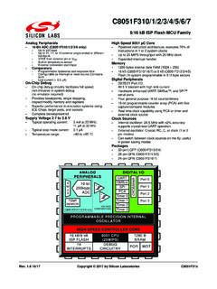
1 Mixed-Signal ISP Flash MCUC8051F330/1/2/3/4/5 Rev. 12/10 Copyright 2010 by Silicon LaboratoriesC8051F330/1/2/3/4/5 Analog Peripherals-10-Bit ADC ( F330/2/4 only) Up to 200 ksps Up to 16 external single-ended or differential inputs VREF from internal VREF, external pin or VDD Internal or external start of conversion source Built-in temperature sensor-10-Bit Current Output DAC ( F330 only)-Comparator Programmable hysteresis and response time Configurable as interrupt or reset source Low current ( A)On-Chip Debug-On-chip debug circuitry facilitates full speed, non-intrusive in-system debug (no emulator required)-Provides breakpoints, single stepping, inspect/modify memory and registers-Superior performance to emulation systems using ICE-chips, target pods, and sockets-Low cost, complete development kitSupply Voltage to V-Typical operating current: mA at 25 MHz.
2 9 A at 32 kHz-Typical stop mode current: A Temperature Range: 40 to +85 CHigh Speed 8051 C Core-Pipelined instruction architecture; executes 70% of instructions in 1 or 2 system clocks-Up to 25 MIPS throughput with 25 MHz clock-Expanded interrupt handlerMemory-768 bytes internal data RAM (256 + 512)-8 kB ( F330/1), 4 kB ( F332/3), or 2 kB ( F334/5) Flash; In-system programmable in 512-byte Sec-tors 512 bytes are reserved in the 8 kB devicesDigital Peripherals-17 Port I/O; All 5 V tolerant with high sink current-Hardware enhanced UART, SMBus , and enhanced SPI serial ports-Four general purpose 16-bit counter/timers-16-Bit programmable counter array (PCA) with three capture/compare modules-Real time clock mode using PCA or timer and exter-nal clock sourceClock Sources-Two internal oscillators: MHz with 2% accuracy supports crystal-less UART operation 80/40/20/10 kHz low frequency, low power-External oscillator: Crystal, RC, C, or clock (1 or 2 pin modes)-Can switch between clock sources on-the-fly.
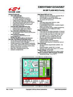
3 Useful in power saving modes20-Pin QFN PackageANALOG PERIPHERALS2/4/8 kB ISP FLASH768 B SRAMPOR DEBUG CIRCUITRYFLEXIBLE INTERRUPTS8051 CPU(25 MIPS)DIGITAL MHz PRECISION INTERNAL OSCILLATORHIGH-SPEED CONTROLLER CORECROSSBARVOLTAGE COMPARATOR+- WDTUARTSMBusPCAT imer 0 Timer 1 Timer 2 Timer 3 Port 0 SPI10-bit Current DACLOW FREQUENCY INTERNAL OSCILLATORPort kspsADCTEMP SENSORAMUX F330/2/4 only F330 onlyC8051F330/1/2/3/4/52 Rev. of Contents1. System CIP-51 Microcontroller Fully 8051 Improved Throughput .. Additional Features .. On-Chip On-Chip Debug Programmable Digital I/O and Crossbar .. Serial Ports .. Programmable Counter Array .. 10-Bit Analog to Digital Comparators .. 10-bit Current Output 302. Absolute Maximum Ratings .. 313. Global Electrical Characteristics .. 324. Pinout and Package 355.
4 10-Bit ADC (ADC0, C8051F330 /2/4 only) .. Analog Multiplexer .. Temperature Sensor .. Modes of Operation .. Starting a Tracking Settling Time Requirements .. Programmable Window Window Detector In Single-Ended Mode .. Window Detector In Differential 546. 10-Bit Current Mode DAC (IDA0, C8051F330 only).. IDA0 Output Scheduling .. Update Output On-Demand .. Update Output Based on Timer Update Output Based on CNVSTR IDAC Output 587. Voltage Reference ( C8051F330 /2/4 only).. 618. Comparator0 .. 659. CIP-51 Microcontroller .. Instruction Set .. Instruction and CPU Timing .. MOVX Instruction and Program Memory .. Memory Program Data General Purpose Bit Addressable 78C8051F330/1/2/3/4/54 Rev. Stack .. Special Function Register Descriptions .. Interrupt Handler.
5 MCU Interrupt Sources and Vectors .. External Interrupts .. Interrupt Priorities .. Interrupt Latency .. Interrupt Register Power Management Modes .. Idle Stop Mode .. 9510. Reset Reset .. Reset/VDD Monitor .. Reset .. Clock Detector Reset .. Reset .. Watchdog Timer Reset .. Error Reset .. Reset .. 10011. Flash Memory .. The Flash Lock and Key Functions .. Erase Procedure .. Write Procedure .. Data Storage .. Options .. Write and Erase Guidelines .. Maintenance and the VDD monitor .. Maintenance .. Clock .. 10812. External RAM .. 11113. Oscillators .. Internal High-Frequency (H-F) Oscillator .. Internal Low-Frequency (L-F) Oscillator .. the Internal L-F Oscillator Drive Crystal RC Capacitor Clock 12114. Port Crossbar Decoder .. I/O Initialization .. 127C8051F330/1/2/3/4/5 Rev.
6 Purpose Port I/O .. 12915. SMBus .. Documents .. Operation .. Low Low High (SMBus Free) Timeout .. the Configuration Control Register .. Register .. Transfer Transmitter Mode .. Receiver Mode .. Receiver Mode .. Transmitter Mode .. Status 15016. Baud Rate Modes .. UART .. UART .. Communications .. 15617. Enhanced Serial Peripheral Interface (SPI0).. Out, Slave In (MOSI).. In, Slave Out (MISO).. Clock (SCK) .. Select (NSS) .. Master Mode Operation .. Slave Mode Operation .. Interrupt Sources .. Clock Special Function Registers .. 16918. 0 and Timer 1 .. 0: 13-bit 1: 16-bit 2: 8-bit Counter/Timer with 3: Two 8-bit Counter/Timers (Timer 0 Only).. 2 .. Timer with 185C8051F330/1/2/3/4/56 Rev. Timers with 3 .. Timer with Timers with 19019.
7 Programmable Counter Array .. Counter/Timer .. Modules .. Capture Timer (Compare) Output Mode .. Output Mode .. Pulse Width Modulator Pulse Width Modulator Timer Mode .. Timer Operation .. Timer Usage .. Descriptions for 20420. C2 Interface .. Interface Pin Sharing .. 211C8051F330/1/2/3/4/5 Rev. of Figures1. System OverviewFigure C8051F330 Block 19 Figure C8051F331 Block 19 Figure C8051F332 Block 20 Figure C8051F333 Block 20 Figure C8051F334 Block 21 Figure C8051F335 Block 21 Figure Comparison of Peak MCU Execution Speeds .. 22 Figure On-Chip Clock and Reset .. 23 Figure On-Board Memory Map .. 24 Figure Development/In-System Debug 25 Figure Digital Crossbar Diagram .. 26 Figure PCA Block 27 Figure PCA Block 27 Figure 10-Bit ADC Block Diagram .. 28 Figure Comparator0 Block Diagram.
8 29 Figure IDA0 Functional Block Diagram .. 302. Absolute Maximum Ratings3. Global Electrical Characteristics4. Pinout and Package DefinitionsFigure QFN-20 Pinout Diagram (Top View).. 375. 10-Bit ADC (ADC0, C8051F330 /2/4 only)Figure ADC0 Functional Block Diagram .. 41 Figure Typical Temperature Sensor Transfer 43 Figure 10-Bit ADC Track and Conversion Example 45 Figure ADC0 Equivalent Input Circuits .. 46 Figure ADC Window Compare Example: Right-Justified Single-Ended 53 Figure ADC Window Compare Example: Left-Justified Single-Ended Data .. 53 Figure ADC Window Compare Example: Right-Justified Differential Data .. 54 Figure ADC Window Compare Example: Left-Justified Differential Data .. 546. 10-Bit Current Mode DAC (IDA0, C8051F330 only)Figure IDA0 Functional Block 57 Figure IDA0 Data Word 587. Voltage Reference ( C8051F330 /2/4 only)Figure Voltage Reference Functional Block Diagram.
9 618. Comparator0 Figure Comparator0 Functional Block 65 Figure Comparator Hysteresis 669. CIP-51 MicrocontrollerFigure CIP-51 Block Diagram .. 71 Figure Memory 7710. Reset SourcesFigure Reset 97C8051F330/1/2/3/4/58 Rev. Power-On and VDD Monitor Reset Timing .. 9811. Flash MemoryFigure Flash Program Memory 10512. External RAM13. OscillatorsFigure Oscillator 113 Figure External kHz Quartz Crystal Oscillator Connection Diagram . 11914. Port Input/OutputFigure Port I/O Functional Block Diagram .. 123 Figure Port I/O Cell Block Diagram .. 124 Figure Crossbar Priority Decoder with No Pins Skipped .. 125 Figure Crossbar Priority Decoder with Crystal Pins Skipped .. 12615. SMBusFigure SMBus Block Diagram .. 135 Figure Typical SMBus Configuration .. 136 Figure SMBus Transaction .. 137 Figure Typical SMBus SCL 141 Figure Typical Master Transmitter 147 Figure Typical Master Receiver 148 Figure Typical Slave Receiver 149 Figure Typical Slave Transmitter 15016.
10 UART0 Figure UART0 Block Diagram .. 153 Figure UART0 Baud Rate Logic .. 154 Figure UART Interconnect 155 Figure 8-Bit UART Timing 155 Figure 9-Bit UART Timing 156 Figure UART Multi-Processor Mode Interconnect Diagram .. 15717. Enhanced Serial Peripheral Interface (SPI0)Figure SPI Block Diagram .. 163 Figure Multiple-Master Mode Connection Diagram .. 166 Figure 3-Wire Single Master and 3-Wire Single Slave Mode Connection Diagram166 Figure 4-Wire Single Master Mode and 4-Wire Slave Mode Connection Diagram166 Figure Master Mode Data/Clock Timing .. 168 Figure Slave Mode Data/Clock Timing (CKPHA = 0) .. 169 Figure Slave Mode Data/Clock Timing (CKPHA = 1) .. 169 Figure SPI Master Timing (CKPHA = 0) .. 173 Figure SPI Master Timing (CKPHA = 1) .. 173 Figure SPI Slave Timing (CKPHA = 0) .. 174 Figure SPI Slave Timing (CKPHA = 1).