Transcription of CD405xB CMOS Single 8-Channel Analog …
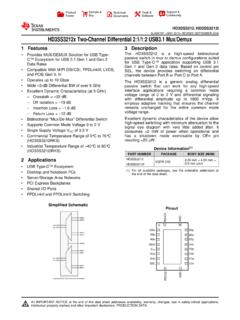
1 Product Order Technical Tools & Support &. Folder Now Documents Software Community CD4051B, CD4052B, CD4053B. SCHS047I AUGUST 1998 REVISED SEPTEMBER 2017. CD405xB CMOS Single 8-Channel Analog Multiplexer/Demultiplexer With Logic-Level Conversion 1 Features 3 Description 1 Wide Range of Digital and Analog Signal Levels The CD405xB Analog multiplexers and demuliplexers are digitally-controlled Analog switches having low Digital: 3 V to 20 V ON impedance and very low OFF leakage current. Analog : 20 VP-P These multiplexer circuits dissipate extremely low Low ON Resistance,125 (Typical) Over 15 VP-P quiescent power over the full VDD VSS and VDD . Signal Input Range for VDD VEE = 18 V VEE supply-voltage ranges, independent of the logic state of the control signals. High OFF Resistance, Channel Leakage of 100. pA (Typical) at VDD VEE = 18 V Device Information(1).
2 Logic-Level Conversion for Digital Addressing PART NUMBER PACKAGE BODY SIZE (NOM). Signals of 3 V to 20 V (VDD VSS = 3 V to 20 V) CDIP (16) mm mm to Switch Analog Signals to 20 VP-P (VDD VEE =. PDIP (16) mm mm 20 V) Matched Switch Characteristics, rON = 5 . CD405xB SOIC (16) mm mm (Typical) for VDD VEE = 15 V Very Low Quiescent SOP (16) mm mm Power Dissipation Under All Digital-Control Input and Supply Conditions, W (Typical) at VDD TSSOP (16) mm mm VSS = VDD VEE = 10 V (1) For all available packages, see the orderable addendum at the end of the data sheet. Binary Address Decoding on Chip 5 V, 10 V, and 15 V Parametric Ratings Functional Diagrams of CD405xB . 100% Tested for Quiescent Current at 20 V. Maximum Input Current of 1 A at 18 V Over Full INH C B A. CBA. Ch 0. Package Temperature Range, 100 nA at 18 V and 000 Ch 1. 001.
3 25 C 010. Ch 2. Break-Before-Make Switching Eliminates Channel COM. 011 Ch 3. 100 Ch 4. Overlap 101. Ch 5. 110. 2 Applications 111 Ch 6. Ch 7. CD4051B. Analog and Digital Multiplexing and Demultiplexing A/D and D/A Conversion INH B A Ch X0. INH. Signal Gating BA. Ch Y0. A ax 00 Ch X1 ax OR ay Factory Automation 01. A ay X COM Ch Y1. Televisions Y COM 10 Ch X2 bx OR by B bx by Appliances 11 Ch Y2. B. cx Consumer Audio Ch X3. cx OR cy C. C cy Programmable Logic Circuits CD4052B. Ch Y3. CD4053B. Sensors 1. An IMPORTANT NOTICE at the end of this data sheet addresses availability, warranty, changes, use in safety-critical applications, intellectual property matters and other important disclaimers. PRODUCTION DATA. CD4051B, CD4052B, CD4053B. SCHS047I AUGUST 1998 REVISED SEPTEMBER 2017 Table of Contents 1 Features .. 1 Feature 17. 2 Applications.
4 1 Device Functional 17. 3 Description .. 1 9 Application and Implementation .. 18. 4 Revision 2 Application 18. Typical Application .. 18. 5 Pin Configuration and Functions .. 3. 6 5 10 Power Supply Recommendations .. 19. Absolute Maximum Ratings .. 5 11 20. ESD 5 Layout Guidelines .. 20. Recommended Operating 5 Layout Example .. 20. Thermal Information .. 5 12 Device and Documentation Support .. 21. Electrical 6 Documentation Support .. 21. AC Performance 8 Related Links .. 21. Typical Characteristics .. 9 Trademarks .. 21. 7 Parameter Measurement Information .. 11 Electrostatic Discharge Caution .. 21. Glossary .. 21. 8 Detailed Description .. 15. Overview .. 15 13 Mechanical, Packaging, and Orderable Functional Block Diagrams .. 15. Information .. 21. 4 Revision History Changes from Revision H (April 2015) to Revision I Page Added: ON Channel Leakage Current to the Electrical Characteristics table.
5 6. Added Note 3 to the Electrical Characteristics table .. 6. Added Figure 13 .. 12. Changes from Revision G (October 2003) to Revision H Page Added Pin Configuration and Functions section, ESD Ratings table, Feature Description section, Device Functional Modes, Application and Implementation section, Power Supply Recommendations section, Layout section, Device and Documentation Support section, and Mechanical, Packaging, and Orderable Information section .. 1. Added Device Information table.. 1. 2 Submit Documentation Feedback Copyright 1998 2017, Texas Instruments Incorporated Product Folder Links: CD4051B CD4052B CD4053B. CD4051B, CD4052B, CD4053B. SCHS047I AUGUST 1998 REVISED SEPTEMBER 2017. 5 Pin Configuration and Functions CD4051B E, M, NS, and PW Package 16-Pin PDIP, CDIP, SOIC, SOP, and TSSOP CD4052B E, M, NS, and PW Package (Top View) 16-Pin PDIP, CDIP, SOP, and TSSOP.
6 (Top View). CHANNELS 4 1 16 VDD. Y CHANNELS 0 1 16 VDD. IN/OUT 6 2 15 2 IN/OUT. 2 2 15 2 X CHANNELS. COM OUT/IN 3 14 1 IN/OUT. CHANNELS IN/OUT COMMON Y OUT/IN 3 14 1. CHANNELS 7 4 13 0. Y CHANNELS 3 4 13 COMMON X OUT/IN. IN/OUT 5 5 12 3 IN/OUT. 1 5 12 0 X CHANNELS. INH 6 11 A IN/OUT. INH 6 11 3. VEE 7 10 B. VEE 7 10 A. VSS 8 9 C. VSS 8 9 B. CD4053B E, M, NS, and PW Package 16-Pin PDIP, CDIP, SOP, and TSSOP. (Top View). by 1 16 VDD. bx 2 15 OUT/IN bx OR by cy 3 14 OUT/IN ax OR ay OUT/IN CX OR CY 4 13 ay IN/OUT. IN/OUT CX 5 12 ax INH 6 11 A. VEE 7 10 B. VSS 8 9 C. Pin Functions CD4051B. PIN. I/O DESCRIPTION. NO. NAME. 1 CH 4 IN/OUT I/O Channel 4 in/out 2 CH 6 IN/OUT I/O Channel 6 in/out 3 COM OUT/IN I/O Common out/in 4 CH 7 IN/OUT I/O Channel 7 in/out 5 CH 5 IN/OUT I/O Channel 5 in/out 6 INH I Disables all channels. See Table 1.
7 7 VEE Negative power input 8 VSS Ground 9 C I Channel select C. See Table 1. 10 B I Channel select B. See Table 1. 11 A I Channel select A. See Table 1. 12 CH 3 IN/OUT I/O Channel 3 in/out 13 CH 0 IN/OUT I/O Channel 0 in/out 14 CH 1 IN/OUT I/O Channel 1 in/out 15 CH 2 IN/OUT I/O Channel 2 in/out 16 VDD Positive power input Copyright 1998 2017, Texas Instruments Incorporated Submit Documentation Feedback 3. Product Folder Links: CD4051B CD4052B CD4053B. CD4051B, CD4052B, CD4053B. SCHS047I AUGUST 1998 REVISED SEPTEMBER 2017 Pin Functions CD4052B. PIN. I/O DESCRIPTION. NO. NAME. 1 Y CH 0 IN/OUT I/O Channel Y0 in/out 2 Y CH 2 IN/OUT I/O Channel Y2 in/out 3 Y COM OUT/IN I/O Y common out/in 4 Y CH 3 IN/OUT I/O Channel Y3 in/out 5 Y CH 1 IN/OUT I/O Channel Y1 in/out 6 INH I Disables all channels. See Table 1. 7 VEE Negative power input 8 VSS Ground 9 B I Channel select B.
8 See Table 1. 10 A I Channel select A. See Table 1. 11 X CH 3 IN/OUT I/O Channel X3 in/out 12 X CH 0 IN/OUT I/O Channel X0 in/out 13 X COM IN/OUT I/O X common out/in 14 X CH 1 IN/OUT I/O Channel in/out 15 X CH 2 IN/OUT I/O Channel in/out 16 VDD Positive power input Pin Functions CD4053B. PIN. I/O DESCRIPTION. NO. NAME. 1 BY IN/OUT I/O B channel Y in/out 2 BX IN/OUT I/O B channel X in/out 3 CY IN/OUT I/O C channel Y in/out CX OR CY. 4 I/O C common out/in OUT/IN. 5 CX IN/OUT I/O C channel X in/out 6 INH I Disables all channels. See Table 1. 7 VEE Negative power input 8 VSS Ground 9 C I Channel select C. See Table 1. 10 B I Channel select B. See Table 1. 11 A I Channel select A. See Table 1. 12 AX IN/OUT I/O A channel X in/out 13 AY IN/OUT I/O A channel Y in/out AX OR AY. 14 I/O A common out/in OUT/IN. BX OR BY. 15 I/O B common out/in OUT/IN.
9 16 VDD Positive power input 4 Submit Documentation Feedback Copyright 1998 2017, Texas Instruments Incorporated Product Folder Links: CD4051B CD4052B CD4053B. CD4051B, CD4052B, CD4053B. SCHS047I AUGUST 1998 REVISED SEPTEMBER 2017. 6 Specifications Absolute Maximum Ratings over operating free-air temperature range (unless otherwise noted) (1). MIN MAX UNIT. Supply Voltage V+ to V-, Voltages Referenced to VSS Terminal 20 V. DC Input Voltage VDD + V. DC Input Current Any One Input 10 10 mA. TJMAX1 Maximum junction temperature, ceramic package 175 C. TJMAX2 Maximum junction temperature, plastic package 150 C. TLMAX Maximum lead temperature, SOIC - Lead Tips Only, Soldering 10s 265 C. Tstg Storage temperature 65 150 C. (1) Stresses beyond those listed under Absolute Maximum Ratings may cause permanent damage to the device. These are stress ratings only, which do not imply functional operation of the device at these or any other conditions beyond those indicated under Recommended Operating Conditions.
10 Exposure to absolute-maximum-rated conditions for extended periods may affect device reliability. ESD Ratings VALUE UNIT. CD4051B in PDIP, CDIP, SOIC, SOP, TSSOP Packages Human-body model (HBM), per ANSI/ESDA/JEDEC JS-001 (1) +3000. V(ESD) Electrostatic discharge Charged-device model (CDM), per JEDEC specification JESD22- V. +2000. C101 (2). CD4053B in PDIP, CDIP, SOP and TSSOP Packages Human-body model (HBM), per ANSI/ESDA/JEDEC JS-001 (1) +2500. V(ESD) Electrostatic discharge Charged-device model (CDM), per JEDEC specification JESD22- V. +1500. C101 (2). (1) JEDEC document JEP155 states that 500-V HBM allows safe manufacturing with a standard ESD control process. (2) JEDEC document JEP157 states that 250-V CDM allows safe manufacturing with a standard ESD control process. Recommended Operating Conditions over operating free-air temperature range (unless otherwise noted).