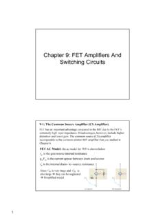
Transcription of Chapter 10: Amplifiers Frequency Response
1 1 Chapter 10: Amplifiers Frequency Response10-1: Basic Concepts Frequency Response of an amplifier is the change in gain or phase shift over a specified range of input signal frequencies In Amplifiers , the coupling and bypass capacitors appear to be shorts to ac at the midband frequencies. At low frequencies the capacitive reactance, XC, of these capacitors affect the gain and phase shift of signals, so they must be taken into of Coupling Capacitors At lower f(10Hz for example) the XCis higher, and it decreases as fincreases more signal voltage is dropped across C1and C3in Amplifiers circuits less voltage gain210-1: Basic ConceptsAlso, a phase shift is introduced by the coupling capacitors because C1forms a lead circuitwith the Rinof the amplifier and C3forms a lead circuit with RLin series with RCor RD. lead circuit is an RC circuit in which the output voltage across R leads the input voltage in phase ; ac voltage signal will be divided between Cand R.
2 Cmakes a phase difference of 90 between current and voltage across no phase difference between current and R we will have VR VC this will cause a phase shift (some where between 0 and 90 ) between input voltage and output voltage of the RCcircuit Composite voltage as result of VRand VCVR = I RVC = I XC10-1: Basic ConceptsEffect of Bypass Capacitors At lower f, the XC2becomes significant large and the emitter (or FET source terminal) is no longer at ac ground. XC2in parallel with RE(or RS) creates an impedance that reduces the gain. Instead ofAt XC>> 0At XC 0310-1: Basic ConceptsOutput Capacitance Cob; between Band Cinput Capacitance Cib; between B and EReverse transfer Capacitance Crss; between Gand Dinput Capacitance Ciss; between Gand S At lower f, the internal capacitances have a very high XC like opens and have no effect on the transistor s performance.
3 However, as the Frequency goes up (at high f), the internal capacitive reactances go down they have a significant effect on the transistor s gain and also it introduces a phase shift; it has the inverse effect to the coupling capacitorsEffect of Internal Transistor Capacitances10-1: Basic ConceptsEffect of Internal Transistor Capacitances When the reactance of Cbe(or Cgs) becomes small enough, a significant amount of the signal voltage is lost due to a voltage-divider effect of thesignal source resistance and the reactance of Cbe. When the reactance of Cbc(or Cgd) becomes small enough, a significant amount of output signal voltage (Vfb) is fed back out of phase with the input (negative feedback) reducing the voltage gain. 410-1: Basic Concepts is used to simplify the analysis of inverting Amplifiers at high frequencies, where the internal transistor capacitances are important The capacitance Cbcin BJTs (Cgdin FETs) between the input and the output is shown in Figure (a) in a generalized form.
4 Where Av is the absolute voltage gain of the inverting amplifier at midrange frequencies, and C represents either Cbcor CgdMiller s Theorem Miller s theorem states that C effectively appears as a capacitance from input to ground, as shown in Figure (b), that can be expressed as follows:Miller s theorem also states that C effectively appears as a capacitance from output to ground, that can be expressed as follows:10-1: Basic ConceptsMiller s Theorem The figure below shows the effective input and output capacitance appears in the actual ac equivalent circuitin parallel with Cbe(or Cgs). Cin(Miller)formula shows that Cbc(or Cgd) has a much greater impact on input capacitance than its actual value. For example, if Cbc6 pF and the amplifier gain is 50, then Cin(Miller) = C(Av+1) = 306 pF. Cout(Miller) indicates that if the voltage gain is 10 or greater Cout(Miller) Cbcor Cgdbecause (Av+1) /Av 1510-2: The Decibel As stated before, The decibel (dB) is a unit of logarithmic gain measurement and is commonly used to express amplifier Response .
5 The decibel is a measurement of the ratio of one power to another or one voltage to power gain in dB is:inoutpPPA=whereThe voltage gain in dB is:inoutvVVA=where If Av > 1 dB gain is positive. If Av< 1 dB gain is negative (attenuation). Example:Express each of the following ratios in dB:solution10-2: The Decibel0 dB Reference Many Amplifiers exhibit a maximum gain (often called midrange gain Av(mid)), over a certain range of frequencies and a reduced gain at frequencies below and above this range. We can assign this maximum gain at midrange to a zerodB reference by setting this maximum gain to 1 into the log by using a ratio with respect to midrange gain (20 log Av/Av(mid) ):For Av(mid) the ratio Av(mid)/Av(mid)= 1 20 log 1 = 0 dB (reference 0 dB). Any other voltage gain below Av(mid)(for same input voltage) will have a ve value. reduction of voltage gain with respect to the maximum (log Av/Av(mid)is -ve) On the other hand, Any other voltage gain above Av(mid)(for same input voltage) will have a +ve value.
6 Increase of voltage gain with respect to the maximum (log Av/Av(mid)is +ve)610-2: The Decibel0 dB ReferenceFor example if Av(mid) = 100 20 log 100/100 = 0 dB is the referenceIf Av = 50 (Av= Av(mid)) 20 log 50/100 = -6 dBIf Av = 25(Av = Av(mid)) 20 log 25/100 = -12 dBIf Av = (Av= Av(mid)) 20 log = -18 dB As you can see (also from table), Halving the output voltage for a steady input voltage is always a 6 dB reduction (-6 dB) in the gain. Correspondingly, a doubling of the output voltage is always a 6 dB increase(+6 dB) in the gain10-2: The DecibelCritical Frequency A critical Frequency (also known as cutoff Frequency or corner Frequency ) is a Frequency at which Poutdrops to one-half (50%) of its P(mid) (at 3 dB reduction in the power gain) Also, at the critical frequencies the voltage gain is of its midrange value and is expressed in dB as(at 3 dB reduction in the voltage gain)Example: A certain amplifier has a midrange rms output voltage of 10 V.
7 What is the rms output voltage for each of the following dB gain reductions with a constant rms input voltage? (a) 3 dB (b) 6 dB (c) 12 dB (d) 24 )/log(20/3)/log(2033))()(20/3)()(== == = = Also you can have dB values from table or figure before710-2: The DecibelPower Measurement in dBm The dBmis a unit for measuring power levels referenced to 1 mW (0 dBm) For +ve dBm power levels above 1 mW For ve dBm power levelsbelow 1 mW. the table shows the dBm values when halved or doubled: As you can see from table, Halving the output power for a steady input voltage is always a 3 dBmreduction (-3 dBm) in the gain. Correspondingly, a doubling of the output power is always a 3 dBmincrease(+3 dB) in the gain10-3: Low Frequency Amplifier Response As descriped before, The voltage gain and phase shift (reduction in voltage gain and an increase in phase shift) of capacitivelycoupled Amplifiers are affected when the signal Frequency is below a critical value.
8 BJT Amplifiers :A typical capacitively coupled CE amplifier is shownAt midrange Frequency , the midrange voltage gainIf a swamping resistor (RE1) is used8 For Frequency below midrange Frequency low Frequency ac equivalent circuit will contain the capacitors C1, C2, and C3 There are three high-pass RC circuits that affect its gain;Ahigh-pass RC circuitan RC circuit passes high- Frequency signals but attenuates reduces the amplitude of signals with frequencies lower than the cutoff Frequency (midrange Frequency ) The three high-pass RC circuits are:RinC1, Rin(emitter)C2, and RoutC3 Resistance looking at the collectorinput resistance ofthe amplifierresistance looking in at the emitter10-3: Low Frequency Amplifier ResponseBJT Amplifiers :BJT Amplifier: The Input RC Circuitdue to XC1, Vbaseis less than voltage at midrange Frequency (Vbase= Vinwhen XC1 0)Lower Critical Frequency Critical point in the amplifier s Response occurs when the Voutis of its midrange value.
9 This may occurs at Vbase= Vin(when Rin= XC1)than at midrange10-3: Low Frequency Amplifier Response9 The Input RC Circuit: Lower Critical Frequency Input lower critical Frequency (or lower cutoff Frequency ), can be calculated as follows:If the resistance of the input source (RS) is taken into account10-3: Low Frequency Amplifier ResponseExample: For the circuit shown, calculate the lower critical Frequency due to the input RC circuit. Assumed r e= and = 200. Notice that a swamping resistor, RE1, is used. The lower critical Frequency is10-3: Low Frequency Amplifier ResponseThe Input RC Circuit: Lower Critical Frequency10 The Input RC Circuit: Voltage Gain Roll-Off at Low Frequencies When the Frequency is reduced to the critical value fc Avof an amplifier is reduced by 3 dB. As the Frequency continues to decrease below fc, Avalso continues to decrease.
10 The rate of decrease Avwith Frequency is called roll-offFor example at f = XC1= 10 Rin Vbasedecrease by 10 times with respect to Vinwhen fdecrease by a decade (10 time)Which corresponds to attenuation10-3: Low Frequency Amplifier ResponseThe Input RC Circuit: Voltage Gain Roll-Off at Low FrequenciesBode plot. (Blue is ideal; red is actual.) For every 10 times change in Frequency f(decade), there is a 20dB decrease in the voltage gain as shown in the following Bode plotExample: The midrange voltage gain of a certain amplifier is 100. The input RC circuit has a lower critical Frequency of 1 kHz. Determine the actual voltage gain at f 1 kHz, f 100 Hz, and f 10 f = fc=1kHz Av= Av(mid)= f = fc=100 Hz Av= Av(mid)=10at f = fc=10 Hz Av= Av(mid)=110-3: Low Frequency Amplifier Response11 The Input RC Circuit: Phase Shift in the Input RC Circuit the phase shift angle of the input RC circuit is expressed as The result is that the voltage at the base of the transistor leads the input signal voltage in phase below midrange10-3: Low Frequency Amplifier ResponseThe Output RC Circuit10-3: Low Frequency Amplifier Response The second high-pass RC circuit in the BJT amplifier is formed by the coupling capacitor C3, the resistance looking in at the collector, and the load resistance RL, as shown belowSource transformation The critical Frequency isThe phase shift angle isThevenin equivalent circuit12 Example.