Transcription of Click 600/601 o-oise ig-recision Series Voltage References
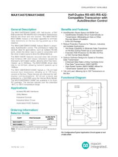
1 19-6355; Rev 18; 12/20 General DescriptionThe MAX6070/MAX6071 offer a very low noise and low-drift Voltage reference in a small 6-pin SOT23 package. These devices provide a 1/f noise Voltage of only VP-P at an output Voltage of , with a temperature drift of 6ppm/ C (max, A grade). The devices consume 150 A of supply current and can sink and source up to 10mA of load current. The low-drift and low-noise specifi-cations enable enhanced system accuracy, making these devices ideal for high-precision industrial applications. The MAX6070 offers a noise filter option for wideband devices are available in a 6-pin SOT23 package and are specified over the extended industrial temperature range of -40 C to +125 C. The options are also available in a 6-bump x wafer-level package (WLP).Applications High-Accuracy Industrial and Process Control Precision Instrumentation High-Resolution ADCs and DACs Precision Current Sources AutomotiveBenefits and Features 6-Pin SOT23 Package Reduces System Board Space Stable Performance over Temperature and Time Improves System Accuracy High Initial Accuracy Low C (typ), 6ppm/ C (max, A grade) Temperature Drift Low VP-P Noise ( to 10Hz) at Low 200mV Dropout Voltage High 85dB Ripple Rejection Low 150 A Supply Current Reduces Power Consumption Filter Option Lowers High-Frequency Noise Output Options.
2 , , , , , , , and Cover Common Voltage Levels for a Wide Variety of Applications x WLP with Bump Spacing AEC-Q100 Qualified (Refer to Ordering Information)Ordering Information and Selector Guide appear at end of data FINENSHUTDOWNCONTROLVINRLOUTFOUTSVOUTMAX 6070 MAX6071 Typical Operating CircuitsMAX6070/MAX6071 Low-Noise, High-Precision Series Voltage ReferencesEVALUATION KIT AVAILABLEC lick here for production status of specific part to GNDS, GNDF, GND .. to the lower of (VIN + ), +6 VOUTS to GNDS, GNDF, GND .. to +6 VIN to GNDS, GNDF, GND .. to +6 VEN to GNDS, GNDF, GND .. to +6 VFILTER to GND .. to the lower of (VIN + ), +6 VGNDS to GNDF .. to + Power Dissipation (TA = +70 C) SOT23 (derate above +70 C) .. WLP (derate above 70 C ..816mWOperating Temperature Range.)
3 -40 C to +125 CJunction Temperature ..+150 CStorage Temperature Range ..-65 C to +150 CSoldering Temperature (reflow) ..+260 CLead Temperature (soldering, 10s) ..+300 C6 SOT23 PACKAGE CODEU6+5/U6+5 AOutline Number21-0058 Land Pattern Number90-0175 Thermal Resistance, Multi-Layer Board:Junction to Ambient ( JA)230 C/WJunction to Case ( JC)76 C/W6 Thin WLPPACKAGE CODEN60B1+1 Outline Number21-0744 Land Pattern NumberRefer to Application Note 1891 Thermal Resistance, Multi-Layer Board:Junction to Ambient ( JA)98 C/WPackage thermal resistances were obtained using the method described in JEDEC specification JESD51-7, using a four-layer board. For detailed information on package thermal considerations, refer to the latest package outline information and land patterns (footprints), go to Note that a + , # , or - in the package code indicates RoHS status only. Package drawings may show a different suffix character, but the drawing pertains to the package regardless of RoHS InformationAbsolute Maximum RatingsStresses beyond those listed under Absolute Maximum Ratings may cause permanent damage to the device.
4 These are stress ratings only, and functional operation of the device at these or any other conditions beyond those indicated in the operational sections of the specifications is not implied. Exposure to absolute maximum rating conditions for extended periods may affect device Integrated 2 MAX6070/MAX6071 Low-Noise, High-Precision Series Voltage References (VIN = + , IOUT = 0mA, COUT = F, TA = -40 C to +125 C, unless otherwise noted. Typical values are at TA = +25 C.) (Note 1)PARAMETERSYMBOLCONDITIONSMINTYPMAXUNIT SOUTPUTO utput Voltage AccuracyMAX6070A/MAX6071A, TA = +25 + , TA = +25 + , TA = +25 + Voltage Temperature Drift (Note 2)TCVOUTMAX6070 CMAX6070 RegulationOver specified VIN rangeTA = +25 C13100 V/VTA = TMIN to TMAX125 Load Regulation0mA < IOUT < 10mA, sink70150 V/mA0mA < IOUT < 10mA, source100150 Output CurrentIOUT-10+10mAShort-Circuit CurrentISCS ourcing to ground25mASinking from VIN25 Long-Term Stability1000 hours at TA = +25 C35ppmThermal Hysteresis(Note 4)
5 85ppmDYNAMIC CHARACTERISTICSN oise VoltageeOUT1/f noise, to 10Hz, COUT = VP-PMAX6071 thermal noise, 10Hz to 10kHz, COUT = VRMSMAX6070 thermal noise, 10Hz to 10kHz,COUT = F, CFILTER = RejectionFrequency = 60Hz100dBTurn-On Settling TimetRSettling to , COUT = FMAX6070, CFILTER = F6msMAX607120 sEnable Settling TimetENSettling to , COUT = FMAX6070, CFILTER = F6msMAX607160 sCapacitive-Load Stability RangeIOUT FINPUTS upply Voltage VING uaranteed by line Supply CurrentIINTA = +25 C130200 ATA = TMIN to TMAX260 Shutdown Supply Current ISD6 AENABLEE nable Input CurrentIEN-1+1 AEnable x VINVE nable x VINE lectrical Characteristics MAX607__AUT12 (VOUT = ) Integrated 3 MAX6070/MAX6071 Low-Noise, High-Precision Series Voltage References (VIN = + , IOUT = 0mA, COUT = F, TA = -40 C to +125 C, unless otherwise noted. Typical values are at TA = +25 C.) (Note 1)PARAMETERSYMBOLCONDITIONSMINTYPMAXUNIT SOUTPUTO utput Voltage AccuracyMAX6070A/MAX6071A, TA = +25 + , TA = +25 + Voltage Temperature Drift (Note 2)TCVOUTMAX6070 CMAX6070 RegulationOver specified VIN rangeTA = +25 C35150 V/VTA = TMIN to TMAX200 Load Regulation0mA < IOUT < 10mA, sink120200 V/mA0mA < IOUT < 10mA, source120200 Output CurrentIOUT-10+10mAShort-Circuit CurrentISCS ourcing to ground25mASinking from VIN25 Long-Term Stability1000 hours at TA = +25 C35ppmThermal Hysteresis(Note 4)
6 85ppmDYNAMIC CHARACTERISTICSN oise VoltageeOUT1/f noise, to 10Hz, COUT = F6 VP-PMAX6071 thermal noise, 10Hz to 10kHz COUT = F7 VRMSMAX6070 thermal noise, 10Hz to 10kHzCOUT = F, CFILTER = F5 Ripple RejectionFrequency = 60Hz89dBTurn-On Settling TimetRSettling to = FMAX6070 CFILTER = F6msMAX607132 sEnable Settling TimetENSettling to = FMAX6070 CFILTER = F6msMAX607160 sCapacitive-Load Stability RangeIOUT FINPUTS upply Voltage VING uaranteed by line Supply CurrentIINTA = +25 C130200 ATA = TMIN to TMAX260 Shutdown Supply Current ISD6 AENABLEE nable Input CurrentIEN-11 AEnable x VINVE nable x VINE lectrical Characteristics MAX607__AUT18 (VOUT = ) Integrated 4 MAX6070/MAX6071 Low-Noise, High-Precision Series Voltage References (VIN = + , IOUT = 0mA, COUT = F, TA = -40 C to +125 C, unless otherwise noted. Typical values are at TA = +25 C.) (Note 1)PARAMETERSYMBOLCONDITIONSMINTYPMAXUNIT SOUTPUTO utput Voltage AccuracyMAX6070A/MAX6071A, TA = +25 + , TA = +25 + Voltage Temperature Drift (Note 2)TCVOUTMAX6070 CMAX6070 RegulationOver specified VIN rangeTA = +25 C50180 V/VTA = TMIN to TMAX225 Load Regulation0mA < IOUT < 10mA, sink135225 V/mA0mA < IOUT < 10mA, source135225 Output CurrentIOUT-10+10mAShort-Circuit CurrentISCS ourcing to ground25mASinking from VIN25 Long-Term Stability1000 hours at TA = +25 C35ppmThermal Hysteresis(Note 4)
7 85ppmDYNAMIC CHARACTERISTICSN oise VoltageeOUT1/f noise, to 10Hz, COUT = VP-PMAX6071 thermal noise, 10Hz to 10kHz COUT = VRMSMAX6070 thermal noise, 10Hz to 10kHzCOUT = F, CFILTER = RejectionFrequency = 60Hz86dBTurn-On Settling TimetRSettling to = FMAX6070 CFILTER = sEnable Settling TimetENSettling to = FMAX6070 CFILTER = sCapacitive-Load Stability RangeIOUT FINPUTS upply VoltageVING uaranteed by line Supply CurrentIINTA = +25 C130200 ATA = TMIN to TMAX260 Shutdown Supply Current ISD6 AENABLEE nable Input CurrentIEN-1+1 AEnable x VINVE nable x VINE lectrical Characteristics MAX607__AUT21 (VOUT = ) Integrated 5 MAX6070/MAX6071 Low-Noise, High-Precision Series Voltage References (VIN = + , IOUT = 0mA, COUT = F, TA = -40 C to +125 C, unless otherwise noted. Typical values are at TA = +25 C.) (Note 1)PARAMETERSYMBOLCONDITIONSMINTYPMAXUNIT SOUTPUTO utput Voltage AccuracyMAX6070A/MAX6071A, TA = +25 + , TA = +25 + , TA = +25 + Voltage Temperature Drift (Note 2)TCVOUTMAX6070 CMAX6070 RegulationOver specified VIN rangeTA = +25 C60145 V/VTA = TMIN to TMAX175 Load Regulation0mA < IOUT < 10mA, sink80140 V/mA0mA < IOUT < 10mA, source75125 Dropout VoltageIOUT = 10mA, TA = TMIN to TMAX (Note 3)110230mVOutput CurrentIOUT-10+10mAShort-Circuit CurrentISCS ourcing to ground25mASinking from VIN25 Long-Term Stability1000 hours at TA = +25 C40ppmThermal Hysteresis(Note 4)
8 85ppmDYNAMIC CHARACTERISTICSN oise VoltageeOUT1/f noise, to 10Hz, COUT = VP-PMAX6071 thermal noise, 10Hz to 10kHz, COUT = F6 VRMSMAX6070 thermal noise, 10Hz to 10kHz, COUT = F, CFILTER = F3 Noise Spectral DensityMAX6071 thermal noise, f = 1kHz, COUT = F60nV/ HzMAX6070 thermal noise, f = 1kHz, COUT = F, CFILTER = F30 Ripple RejectionFrequency = 60Hz84dBTurn-On Settling TimetRSettling to , COUT = FMAX6070, CFILTER = F10msMAX607130 sEnable Settling TimetENSettling to , COUT = FMAX6070, CFILTER = F10msMAX607175 sCapacitive-Load Stability RangeIOUT FINPUTS upply Voltage VING uaranteed by line Supply CurrentIINTA = +25 C150235 ATA = TMIN to TMAX300 Shutdown Supply Current AElectrical Characteristics MAX607__AUT25 (VOUT = ) Integrated 6 MAX6070/MAX6071 Low-Noise, High-Precision Series Voltage References (VIN = + , IOUT = 0mA, CIN = COUT = F, TA = 0 C to +85 C, unless otherwise noted. Typical values are at TA = +25 C.)
9 (Note 1)(VIN = + , IOUT = 0mA, COUT = F, TA = -40 C to +125 C, unless otherwise noted. Typical values are at TA = +25 C.) (Note 1)PARAMETERSYMBOLCONDITIONSMINTYPMAXUNIT SENABLE/SHUTDOWNE nable Input CurrentIEN-1+1 AEnable x VINVE nable x VINPARAMETERSYMBOLCONDITIONSMINTYPMAXUNI TSOUTPUTO utput Voltage AccuracyTA = +25 + Voltage Temperature Drift (Note 2) CLine RegulationOver specified VIN rangeTA = +25 C60300 V/VTA = TMIN to TMAX350 Load Regulation0mA < IOUT < 10mA, sink80200 V/mA0mA < IOUT < 10mA, source75180 Dropout VoltageIOUT = 10mA, TA = TMIN to TMAX (Note 3)110230mVOutput CurrentIOUT-10+10mAShort-Circuit CurrentISCS ourcing to ground25mASinking from VIN25 Long-Term Stability1000 hours at TA = +25 C16ppmThermal Hysteresis(Note 4)85ppmDYNAMIC CHARACTERISTICSN oise VoltageeOUT1/f noise, to 10Hz, COUT = VP-P10Hz to 10kHz, COUT = F6 VRMSN oise Spectral DensityfSW = 1kHz, COUT = F60nV/ HzRipple RejectionFrequency = 60Hz84dBTurn-On Settling TimetRSettling to , COUT = F30 sEnable Settling TimetENSettling to , COUT = F75 sCapacitive-Load Stability RangeIOUT FINPUTS upply Voltage VING uaranteed by line Supply CurrentIINTA = +25 C160250 ATA = TMIN to TMAX320 Shutdown Supply Current AENABLE/SHUTDOWNE nable Input CurrentIEN-1+1 AEnable x VINVE nable x VINE lectrical Characteristics MAX607__ANT25 (VOUT = )Electrical Characteristics MAX607__AUT25 (VOUT = ) (continued) Integrated 7 MAX6070/MAX6071 Low-Noise, High-Precision Series Voltage References (VIN = + , IOUT = 0mA, COUT = F, TA = -40 C to +125 C, unless otherwise noted.)
10 Typical values are at TA = +25 C.) (Note 1)PARAMETERSYMBOLCONDITIONSMINTYPMAXUNIT SOUTPUTO utput Voltage AccuracyMAX6070A/MAX6071A, TA = +25 + , TA = +25 + , TA = +25 + Voltage Temperature Drift (Note 2)TCVOUTMAX6070 CMAX6070 RegulationOver specified VIN rangeTA = +25 C90200 V/VTA = TMIN to TMAX260 Load Regulation0mA < IOUT < 10mA, sink90170 V/mA0mA < IOUT < 10mA, source90150 Dropout VoltageIOUT = 10mA, TA = TMIN to TMAX (Note 3)80150mVOutput CurrentIOUT-10+10mAShort-Circuit CurrentISCS ourcing to ground25mASinking from VIN25 Long-Term Stability1000 hours at TA = +25 C40ppmThermal Hysteresis(Note 4)85ppmDYNAMIC CHARACTERISTICSN oise VoltageeOUT1/f noise, to 10Hz, COUT = VP-PMAX6071 thermal noise, 10Hz to 10kHz, COUT = VRMSMAX6070 thermal noise, 10Hz to 10kHz, COUT = F, CFILTER = RejectionFrequency = 60Hz80dBTurn-On Settling TimetRSettling to , COUT = FMAX6070, CFILTER = sEnable Settling TimetENSettling to , COUT = FMAX6070, CFILTER = sCapacitive-Load Stability RangeIOUT FINPUTS upply Voltage VING uaranteed by line Supply CurrentIINTA = +25 C150235 ATA = TMIN to TMAX300 Shutdown Supply Current AENABLE/SHUTDOWNE nable Input CurrentIEN-1+1 AEnable x VINVE nable x VINE lectrical Characteristics MAX607__AUT30 (VOUT = ) Integrated 8 MAX6070/MAX6071 Low-Noise, High-Precision Series Voltage References (VIN = + , IOUT = 0mA, COUT = F, TA = -40 C to +125 C, unless otherwise noted.

