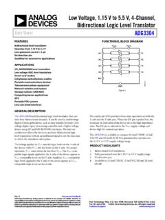
Transcription of CMOS, 1.8 V to 5.5 V/±2.5 V, 3 Ω Low Voltage 4-/8 …
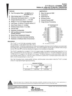
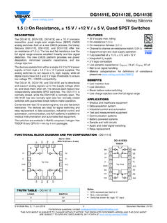
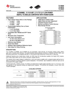
1 CMOS, V to V/ V, 3 Low Voltage 4-/8- channel Multiplexers data sheet adg708 / adg709 FEATURES V to V single supply V dual supply 3 on resistance on resistance flatness 100 pA leakage currents 14 ns switching times Single 8-to-1 multiplexer adg708 Differential 4-to-1 multiplexer adg709 16-lead TSSOP package Low power consumption TTL-/CMOS-compatible inputs Qualified for automotive applications APPLICATIONS data acquisition systems Communication systems Relay replacement Audio and video switching Battery-powered systems GENERAL DESCRIPTION The adg708 / adg709 are low Voltage , CMOS analog multiplexers comprising eight single channels and four differential channels, respectively.
2 The adg708 switches one of eight inputs (S1 to S8) to a common output, D, as determined by the 3-bit binary address lines A0, A1, and A2. The adg709 switches one of four differential inputs to a common differential output as determined by the 2-bit binary address lines A0 and A1. An EN input on both devices is used to enable or disable the device. When disabled, all channels are switched off. Low power consumption and an operating supply range of V to V make the adg708 / adg709 ideal for battery-powered, portable instruments. All channels exhibit break-before-make switching action preventing momentary shorting when switching channels.
3 These switches are designed on an enhanced submicron process that provides low power dissipation yet gives high switching speed, very low on resistance, and leakage currents. On resistance is in the region of a few ohms and is closely matched between switches and very flat over the full signal range. These parts can operate equally well as either multiplexers or demultiplexers and have an input signal range that extends to the supplies. FUNCTIONAL BLOCK DIAGRAMS S1S8A0DA1A2 ADG708EN1 OF 8 DECODER00041-001 Figure 1. S1AA0 DAS4AS1BS4 BDBENADG7091 OF 4 DECODERA100041-002 Figure 2. PRODUCT HIGHLIGHTS 1. Single-/dual-supply operation.
4 The adg708 / adg709 are fully specified and guaranteed with 3 V and 5 V single-supply and V dual-supply rails. 2. Low RON (3 typical). 3. Low power consumption (< W). 4. Guaranteed break-before-make switching action. 5. Small 16-lead TSSOP package. The adg708 / adg709 are available in a 16-lead TSSOP. Rev. E Document Feedback Information furnished by Analog Devices is believed to be accurate and reliable. However, no responsibility is assumed by Analog Devices for its use, nor for any infringements of patents or other rights of third parties that may result from its use. Specifications subject to change without notice.
5 No license is granted by implication or otherwise under any patent or patent rights of Analog Devices. Trademarks and registered trademarks are the property of their respective owners. One Technology Way, Box 9106, Norwood, MA 02062-9106, Tel: 2000 2014 Analog Devices, Inc. All rights reserved. Technical Support adg708 / adg709 data sheet TABLE OF CONTENTS Features .. 1 Applications .. 1 General Description .. 1 Functional Block Diagrams .. 1 Product Highlights .. 1 Revision History .. 2 Specifications .. 3 Dual Supply .. 7 Absolute Maximum Ratings .. 9 ESD Caution .. 9 Pin Configurations and Function Descriptions.
6 10 Tr u t h Ta b l e 11 Typical Performance Characteristics .. 12 Test Circuits .. 15 Terminology .. 18 Applications Information .. 19 Power Supply Sequencing .. 19 Outline Dimensions .. 20 Ordering Guide .. 20 Automotive Products .. 20 REVISION HISTORY 9/14 Rev. D to Rev. E Changes to Ordering Guide .. 20 1/13 Rev. C to Rev. D Changes to Ordering Guide .. 20 4/09 Rev. B to Rev. C Changes to Table 1 .. 3 Changes to Table 2 .. 5 Changes to Table 3 .. 7 Mo v e d Tr u t h Ta b l e s Section .. 11 Changes to Figure 7, Figure 8, and Figure 12 Changes to Figure 13 and Figure 14 .. 13 Moved Terminology Section .. 18 Changes to Ordering Guide.
7 20 8/06 Rev. A to Rev. B Updated Format .. Universal Changes to Absolute Maximum Ratings Section .. 9 Added Table 7 and Table 8 .. 10 Updated Outline Dimensions .. 18 Changes to Ordering Guide .. 18 4/02 Rev. 0 to Rev. A Edits to Features and Product Highlights .. 1 Change to Specifications .. 2 4 Edits to Absolute Maximum Ratings Notes .. 5 Edits to TPCs 2, 5, 6 9, 11, and 15 .. 7 9 Edits to Test Circuits 9 and 10 .. 11 Addition of Test Circuit 11 .. 11 10/00 Revision 0: Initial Version Rev. E | Page 2 of 20 data sheet adg708 / adg709 SPECIFICATIONS VDD = 5 V 10%, VSS = 0 V, GND = 0 V, unless otherwise noted. Table 1.
8 B Version C Version Parameter +25 C 40 C to +85 C 40 C to +125 C +25 C 40 C to +85 C 40 C to +125 C Unit Test Conditions/ Comments ANALOG SWITCH Analog Signal Range 0 V to VDD 0 V to VDD 0 V to VDD V On Resistance (RON) 3 3 typ VS = 0 V to VDD, IDS = 10 mA; see Figure 20 5 7 5 7 max On Resistance Match Between Channels ( RON) typ max VS = 0 V to VDD, IDS = 10 mA On Resistance Flatness (RF L AT (ON)) typ VS = 0 V to VDD, IDS = 10 mA max LEAKAGE CURRENTS VDD = V Source Off Leakage, IS (Off) nA typ VD = V/1 V, VS = 1 V; see Figure 21 20 20 1 nA max Drain Off Leakage, ID (Off) nA typ VD = V/1 V, VS = 1 V; see Figure 22 20 20 6 nA max channel On Leakage, ID, IS (On) nA typ VD = VS = 1 V or V.
9 See Figure 23 20 20 6 nA max DIGITAL INPUTS Input High Voltage , VINH V min Input Low Voltage , VINL V max Input Current IINL or IINH A typ VIN = VINL or VINH A max Digital Input Capacitance, CIN 2 2 pF typ DYNAMIC CHARACTERISTICS1 tTRANSITION 14 14 ns typ RL = 300 , CL = 35 pF; see Figure 24 25 25 25 25 ns max VS1 = 3 V/0 V, VS8 = 0 V/3 V Break-Before-Make Time Delay, tOPEN 8 8 ns typ RL = 300 , CL = 35 pF 1 1 1 1 ns min VS = 3 V; see Figure 25 tON (EN) 14 14 ns typ RL = 300 , CL = 35 pF 25 25 25 25 ns max VS = 3 V; see Figure 26 tOFF (EN) 7 7 ns typ RL = 300 , CL = 35 pF 12 12 12 12 ns max VS = 3 V; see Figure 26 Charge Injection 3 3 pC typ VS = V, RS = 0 , CL = 1 nF; See Figure 27 Off Isolation 60 60 dB typ RL = 50 , CL = 5 pF, f = 10 MHz 80 80 dB typ RL = 50 , CL = 5 p F, f = 1 MHz; see Figure 28 Rev.
10 E | Page 3 of 20 adg708 / adg709 data sheet B Version C Version Parameter +25 C 40 C to +85 C 40 C to +125 C +25 C 40 C to +85 C 40 C to +125 C Unit Test Conditions/ Comments channel -to- channel Crosstalk 60 60 dB typ RL = 50 , CL = 5 p F, f = 10 MHz 80 80 dB typ RL = 50 , CL = 5 p F, f = 1 MHz; see Figure 29 3 dB Bandwidth 55 55 MHz typ RL = 50 , CL = 5 pF; see Figure 30 CS (Off ) 13 13 pF typ f = 1 MHz CD (Off ) adg708 85 85 pF typ f = 1 MHz adg709 42 42 pF typ f = 1 MHz CD, CS (On) adg708 96 96 pF typ f = 1 MHz adg709 48 48 pF typ f = 1 MHz POWER REQUIREMENTS VDD = V IDD A typ Digital inputs = 0 V or V A max 1 Guaranteed by design, not subject to production test.