Transcription of Cree C3M0025065D Silicon Carbide MOSFET
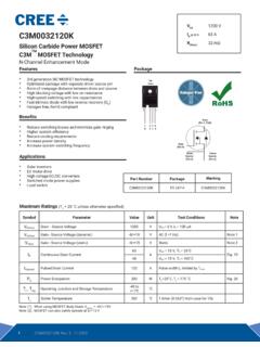
1 1C3M0025065D Rev 1, 12-2020C3M0025065 DSilicon Carbide power MOSFET C3 MTM MOSFET TechnologyN- channel Enhancement Mode Features 3rd Generation SiC MOSFET technology High blocking voltage with low on-resistance High speed switching with low capacitances Fast intrinsic diode with low reverse recovery (Qrr) Halogen free, RoHS compliantBenefits Higher system efficiency Reduced cooling requirements Increased power density Increased system switching frequency Easy to parallel and simple to drive Enable new hard switching PFC topologies (Totem-Pole)Applications EV chargers UPS Solar inverters Industrial SMPS DC/DC converters Package Part NumberPackageMarkingC3M0025065 DTO-247-3C3M0025065D VDS 650 V ID @ 25 C 97 A RDS(on)
2 25 m Maximum RatingsSymbolParameterValueUnitNoteVDSSD rain - Source Voltage, TC = 25 C650 VVGSGate - Source voltage (Under transient events < 100 ns)-8/+19 VFig. 29ID Continuous Drain Current, VGS = 15 V, TC = 25 C97 AFig. 19 Continuous Drain Current, VGS = 15 V, TC = 100 C70ID(pulse)Pulsed Drain Current, Pulse width tP limited by Tjmax 251 APD power Dissipation, TC=25 C, TJ = 175 C326 WFig. 20TJ , TstgOperating Junction and Storage Temperature-40 to +175 CTLS older Temperature, ( ) from case for 10s260 CMdMounting Torque, (M3 or 6-32 screw) Rev 1, 12-2020 Electrical Characteristics (TC = 25 C unless otherwise specified) ConditionsNoteV(BR)DSSD rain-Source Breakdown Voltage650 VVGS = 0 V, ID = 100 AVGSonGate-Source Recommended Turn-On Voltage15 VStatic Fig.
3 29 VGSoffGate-Source Recommended Turn-Off Voltage-4 VVGS(th)Gate Threshold = VGS, ID = mA Fig. = VGS, ID = mA, TJ = 175 CIDSSZero Gate Voltage Drain Current150 AVDS = 650 V, VGS = 0 VIGSSGate-Source Leakage Current10250nAVGS = 15 V, VDS = 0 VRDS(on)Drain-Source On-State Resistance 2534m VGS = 15 V, ID = A Fig. 4, 5,6 33 VGS = 15 V, ID = A, TJ = 175 CgfsTransconductance25 SVDS= 20 V, IDS= A Fig. 724 VDS= 20 V, IDS= A, TJ = 175 CCissInput Capacitance2980pFVGS = 0 V, VDS = 0V to 600 VF = 1 MhzVAC = 25 mV Fig. 17, 18 CossOutput Capacitance178 CrssReverse Transfer Capacitance12Co(er)Effective Output Capacitance (Energy Related)236 VGS = 0 V, VDS = 0V to 400 V Note: 1Co(tr)Effective Output Capacitance (Time Related)340 Note: 1 EossCoss Stored Energy37 JVDS = 600 V, F = 1 Mhz Fig.
4 16 EONTurn-On Switching Energy (Body Diode)578 JVDS = 400 V, VGS = -4 V/15 V, ID = A, RG(ext) = , L= 59 H, TJ = 175 C FWD = Internal Body Diode of MOSFET Fig. 25 EOFFTurn Off Switching Energy (Body Diode)214 EONTurn-On Switching Energy (External Diode)392 JVDS = 400 V, VGS = -4 V/15 V, ID = A, RG(ext) = , L= 59 H, TJ = 175 C FWD = External SiC DIODE Fig. 25 EOFFTurn Off Switching Energy (External Diode)238td(on)Turn-On Delay Time14nsVDD = 400 V, VGS = -4 V/15 VID = A, RG(ext) = Timing relative to VDS Inductive load Fig. 26trRise Time60td(off)Turn-Off Delay Time27tfFall Time 12RG(int)Internal Gate f = 1 MHz, VAC = 25 mVQgsGate to Source Charge29nCVDS = 400 V, VGS = -4 V/15 VID = APer IEC60747-8-4 pg 21 Fig.
5 12 QgdGate to Drain Charge37 QgTotal Gate Charge108 Note (1): Co(er), a lumped capacitance that gives same stored energy as Coss while Vds is rising from 0 to 400V Co(tr), a lumped capacitance that gives same charging time as Coss while Vds is rising from 0 to 400V3C3M0025065D Rev 1, 12-2020 Reverse Diode Characteristics (TC = 25 C unless otherwise specified) ConditionsNoteVSDD iode Forward = -4 V, ISD = A, TJ = 25 CFig. 8, 9, = -4 V, ISD = A, TJ = 175 CISC ontinuous Diode Forward Current52 AVGS = -4 V, TC = 25 CIS, pulseDiode pulse Current251 AVGS = -4 V, pulse width tP limited by TjmaxtrrReverse Recover time33nsVGS = -4 V, ISD = A, VR = 400 Vdif/dt = 745 A/ s, TJ = 175 CQrrReverse Recovery Charge309nCIrrmPeak Reverse Recovery Current17 AtrrReverse Recover time51nsVGS = -4 V, ISD = A, VR = 400 Vdif/dt = 685 A/ s, TJ = 175 CQrrReverse Recovery Charge261nCIrrmPeak Reverse Recovery Current12 AThermal CharacteristicsSymbolParameter ConditionsNoteR JCThermal Resistance from Junction to C/WFig.
6 21R JAThermal Resistance From Junction to Ambient404C3M0025065D Rev 1, 12-2020 Figure 2. Output Characteristics TJ = 25 CTypical PerformanceFigure 5. On-Resistance vs. Drain CurrentFor Various Temperatures Figure 1. Output Characteristics TJ = -40 CFigure 3. Output Characteristics TJ = 175 Resistance, RDS On( )Junction Temperature, Tj( C)Conditions:IDS= AVGS= 15 Vtp< 200 s051015202530354045500204060801001201401 60On Resistance, RDS On(mOhms)Drain-Source Current, IDS(A)Conditions:VGS= 15 Vtp< 200 sTj= 175 CTj= -40 CTj= 25 CFigure 4. Normalized On-Resistance vs. Temperature 010203040506070-50-250255075100125150175 On Resistance, RDS On(mOhms)Junction Temperature, Tj( C)Conditions:IDS= Atp< 200 sVGS= 15 VVGS= 13 VVGS= 11 VFigure 6.
7 On-Resistance vs. TemperatureFor Various Gate Current, IDS(A)Drain-Source Voltage, VDS(V)Conditions:Tj= 175 Ctp =< 200 sVGS= 7 VVGS= 13 VVGS= 11 VVGS= 9 VVGS= Current, IDS(A)Drain-Source Voltage, VDS(V)Conditions:Tj= 25 Ctp =< 200 sVGS= 7 VVGS= 13 VVGS= 11 VVGS= 9 VVGS= Current, IDS(A)Drain-Source Voltage, VDS(V)Conditions:Tj= -40 Ctp =< 200 sVGS= 7 VVGS= 13 VVGS= 11 VVGS= 9 VVGS= 15V5C3M0025065D Rev 1, 12-2020 Typical PerformanceFigure 8. Body Diode Characteristic at -40 CFigure 9. Body Diode Characteristic at 25 C02040608010012014002468101214 Drain-Source Current, IDS(A)Gate-Source Voltage, VGS(V)Conditions:VDS= 20 Vtp <200 sTJ= 25 CTJ= -40 CTJ= 175 C-140-120-100-80-60-40-200-10-8-6-4-20 Drain-Source Current, IDS(A)Drain-Source Voltage VDS(V)Conditions:Tj= -40 Ctp< 200 sVGS= -2 VVGS= -4 VVGS= 0 V-140-120-100-80-60-40-200-10-8-6-4-20 Drain-Source Current, IDS(A)Drain-Source Voltage VDS(V)Conditions:Tj= 25 Ctp< 200 sVGS= -2 VVGS= -4 VVGS= 0 V-140-120-100-80-60-40-200-10-8-6-4-20 Drain-Source Current, IDS(A)Drain-Source Voltage VDS(V)Conditions.
8 Tj= 175 Ctp< 200 sVGS= -2 VVGS= -4 VVGS= 0 Voltage, Vth(V)Junction Temperature TJ( C)ConditonsVGS= VDSIDS= 10. Body Diode Characteristic at 175 C-40481216020406080100120 Gate-Source Voltage, VGS(V)Gate Charge, QG(nC)Conditions:IDS= IGS= 50 mAVDS= TJ= 25 A400 VFigure 7. Transfer Characteristic for Various Junction TemperaturesFigure 11. Threshold Voltage vs. TemperatureFigure 12. Gate Charge Characteristics6C3M0025065D Rev 1, 12-2020 Typical PerformanceFigure 15. 3rd Quadrant Characteristic at 175 CFigure 13. 3rd Quadrant Characteristic at -40 C-140-120-100-80-60-40-200-10-8-6-4-20 Drain-Source Current, IDS(A)Drain-Source Voltage VDS(V)Conditions:Tj= -40 Ctp< 200 sVGS= 10 VVGS= 5 VVGS= 15 VVGS= 0 V-140-120-100-80-60-40-200-10-8-6-4-20 Drain-Source Current, IDS(A)Drain-Source Voltage VDS(V)Conditions:Tj= 25 Ctp< 200 sVGS= 10 VVGS= 5 VVGS= 15 VVGS= 0 V-140-120-100-80-60-40-200-10-8-6-4-20 Drain-Source Current, IDS(A)Drain-Source Voltage VDS(V)Conditions:Tj= 175 Ctp< 200 sVGS= 10 VVGS= 5 VVGS= 15 VVGS= 0 VFigure 14.
9 3rd Quadrant Characteristic at 25 C051015202530354045500100200300400500600 700 Stored Energy, EOSS( J)Drain to Source Voltage, VDS(V)Figure 16. Output Capacitor Stored EnergyFigure 17. Capacitances vs. Drain-Source Voltage (0 - 200V)110100100010000050100150200 Capacitance (pF)Drain-Source Voltage, VDS(V)CissCossConditions:TJ= 25 CVAC= 25 mVf = 1 MHzCrss110100100010000010020030040050060 0700 Capacitance (pF)Drain-Source Voltage, VDS(V)CissCossConditions:TJ= 25 CVAC= 25 mVf = 1 MHzCrssFigure 18. Capacitances vs. Drain-Source Voltage (0 - 650V)7C3M0025065D Rev 1, 12-20201E-310E-3100E-3 11E-610E-6100E-61E-310E-3100E-3 1 Junction To Case Impedance, ZthJC(oC/W)Time, tp(s) Performance0102030405060708090100-50-250 255075100125150175 Drain-Source Continous Current, IDS (DC)(A)Case Temperature, TC( C)Conditions:TJ 175 C050100150200250300350-50-25025507510012 5150175 Maximum Dissipated power , Ptot(W)Case Temperature, TC( C)Conditions:TJ 175 Current, IDS(A)Drain-Source Voltage, VDS(V)100 s1 ms10 sConditions:TC= 25 CD = 0, Parameter: tp100 msLimited by RDS On1 sFigure 22.
10 Safe Operating AreaFigure 21. Transient Thermal Impedance(Junction - Case) Loss (mJ)Drain to Source Current,IDS(A)EOffEOnETotalConditions:TJ = VDD= RG(ext)= VGS= FWD = L = 25 C400 -4/+15 VC3M0025065D59 HFigure 23. Clamped Inductive Switching Energy vs. Drain Current (VDD = 400V)Figure 19. Continuous Drain Current Derating vs. Case TemperatureFigure 20. Maximum power Dissipation Derating vs. Case Loss (mJ)External Gate Resistor RG(ext) (Ohms)EOffEOnETotalConditions:TJ= VDD= IDS= VGS= FWD = L = 25 C400 A-4/+15 VC3M0025065D59 HFigure 24. Clamped Inductive Switching Energy vs. RG(ext)8C3M0025065D Rev 1, 12-2020 Typical Loss (mJ)Junction Temperature, TJ( C)EOffEOnETotalConditions:IDS= VDD= RG(ext)= VGS= L = FWD =FWD = A 400 -4/+15 V59 H C3M0025065 DETotal with SchottkyEOn with SchottkyEOff with SchottkyC3D16065 AFigure 25.