Transcription of Crystal Structure of Graphite, Graphene and Silicon
1 Crystal Structure of graphite , Graphene and SiliconDodd Gray, Adam McCaughan, Bhaskar Mookerji Physics for Solid State Applications(Dated: March 13, 2009)We analyze Graphene and some of the carbon allotropes for which Graphene sheetsform thebasis. The real-space and reciprocal crystalline structures are analyzed. Theoretical X-ray diffrac-tion (XRD) patterns are obtained from this analysis and compared with experimental results. Weshow that staggered two-dimensional hexagonal lattices of graphite haveXRD patterns that differsignificantly from Silicon wide-variety of carbon allotropes and their associ-ated physical properties are largely due to the flexibilityof carbon s valence electrons and resulting dimensionalityof its bonding structures.
2 Amongst carbon-only systems,two-dimensional hexagonal sheets Graphene forms ofthe basis of other important carbon structures such asgraphite and carbon nanotubes. (:: Say something aboutinteresting band Structure here)In the following, we will examine the planar lat-tice Structure of Graphene and its extension to higher-dimensional lattice structures, such as hexagonalgraphite. We first analyze the lattice and reciprocal-space structures of two-dimensional hexagonal lattices ofcarbon, and use the resulting Structure factors to esti-mate the x-ray diffraction (XRD) intensities of conclude by comparing its calculated XRD spectra toexperimental spectra of Graphene and crystalline PRELIMINARY lattice StructureOur discussion of the Crystal Structure of graphite fol-lows partially from Chung s review of graphite [1].
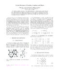
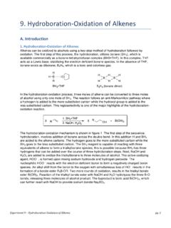
3 When multiple Graphene sheets are layered on top of eachother, van der Walls bonding occurs and the three di-mensional Structure of graphite is formed with a latticeFIG. 1: In-plane Structure of graphite and reciprocal latticevectors [1]. Electronic between sheetsc= A. The sheets align suchthat their two-dimensional hexagonal lattices are stag-gered, either in an ABAB pattern or an ABCABC pat-tern. The ABAB alignment is shown in Figure1, whichindicates four atoms per unit cell labeled A, B, A , andB , respectively. The primed atoms A B on one graphenelayer are separated by half the orthogonal lattice spacingfrom the A B layer; BB atomic pairs differ from theircorresponding AA pairs in their absence of neighboringatoms in adjacent layering planes.
4 The coordinates ofthese atoms forming the basis are given by: A= (0,0,0) A =(0,0,c2) B=a2(1 3,1,0) B =( a2 3, a2,c2)( )With respect to an orthonormal basis, the primitivelattice vectors are given by,a1=a( 3/2, 1/2,0)|a1|=a= Aa2=a( 3/2,1/2,0)|a2|=a= Aa3=c(0,0,1)|a3|=c= A.( )The magnitudes of the primitive lattice vectors corre-spond to the lattice constants parallel and perpendicu-lar to the Graphene sheet. The corresponding ABCABC layer forms a rhombohedral Structure with identical lat-tice spacing parallel and orthogonal to the Reciprocal lattice StructureRecall that the reciprocal lattice vectorsbiare definedas a function of the primitive lattice vectorsaisuch thatb1= 2 a2 a3a1 a3 a3b2= 2 a3 a1a2 a3 a1b3= 2 a1 a2a3 a1 a2( )The reciprocal lattice vectors for graphite are then2 FIG.
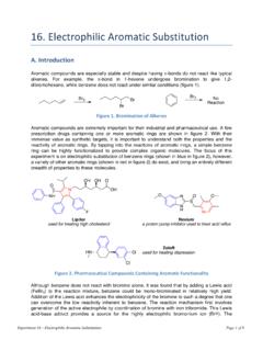
5 2: Reciprocal lattice planes [001], [110], and [111].given by,b1=2 a(1 3, 1,0)|b1|=2 a2 3b2=2 a(1 3,1,0)|b2|=2 a2 3b3=2 c(0,0,1)|b3|=2 c.( )The reciprocal lattice plane generated by theb1andb2vectors forms the outline of the first Brillouin zone, asdepicted in Figure1. The intersection of the the planeskz= 2 /cwith the plane forms a hexagonal prism ofheight 4 Atomic form factorsAs carbon is the only element present in Graphene andgraphite, the atomic form factor is uniform across theentire Crystal , and thus can be factored out when calcu-lating the Structure factor. Thus the atomic form factorhas no effect on the relative intensities of x-ray diffrac-tion occuring in different planes of graphite . Accordingto the NIST Physics Laboratory, the atomic form factorof carbon varies from to e/atom with incidentradiation ranging from 2 to 433 KeV [2].
6 2. X-RAY Planes in the Reciprocal LatticeProvide pictures of the Crystal and of thereciprocal lattice in the [100], [110], and [111]planes. Indicate the vertical positions ofatoms with respect to the of the Crystal and of the reciprocal lattice inthe [100], [110], and [111] planes are included in Fig-ure2. In MATLAB, the Crystal was represented as a setof points in space using the specified lattice vectors andatom bases. Normals generated from lattice vector sumswere used to extract planes and display them. Varyingcolors were used to depict vertical spacing between adja-cent Structure Factors and X-Ray DiffractionIntensitiesCalculate the Structure factor for all thereciprocal lattice vectorsKl<16 (2 /a) Structure factor is calculated asMp(Ki) =fcn j=1(Ki)e iKi iwherefcis the Structure factor of Carbon and iare thebasis vectors of our lattice .
7 We find that only four unique,non-zero values ofMp(Ki) occur in the reciprocal of these corresponds to the height of a diffractionintensity peak and their relative values are referenced the ratio of the intensities ex-pected for the following lines of the diffractionpattern with respect to the [111] line: [100],[200], [220], [311], and [400].Including the Structure factor, there are other severalfactors contributing to the intensities of the diffractionpeaks [3]:1. TheLorenz correctionis a geometric relation al-tering the intensity of an x-ray beam for differentscattering angles .2. Themultiplicity factorpis defined as the num-ber of different planes having the same spacingthrough the unit cell. Systems with high symme-tries will have different planes contributing to thesame diffraction, thereby increasing the , absorption, polarizationeach con-tribute higher-order corrections ultimately ignoredin our calculation.
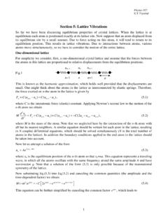
8 These include Doppler broad-ening from thermal vibrations in the material, ab-sorption of x-rays, and the polarization of initiallyunpolarized x-rays upon elastic factors all contribute to the relative intensity of a[hkl] diffraction peak given byI[hkl]( ) =p|Ma(Km)|2(1 + cos22 sin2 cos ).( )Using the formula from the previous question to calcu-late the ratios of the Structure factors in the given planes,3 FIG. 3: Crystal Structure of I: X-Ray diffraction intensities for graphite and sili-con [4,5]. Structure factors are included in ( graphite )2 ( ) ( ) [111] (3) [100] (3) [200] (1) [002] 106 (16)100[220] (1) [311] (3) [400] (1) we obtain the following results presented in TableI. Cal-culations show that planes [100], [200], [220] and [400] ex-hibit relative diffraction intensities 1/3 that of the [111]and [311] planes.
9 The [002] plane exhibits the highest in-tensity diffraction, 16/3 that of the [111] and [311] also found several non-zero Structure factors that arenot present in the experimental Crystal Structure of SiliconWhat are the ratios if the material wereSi? How could you use this information todistinguish Si from your material by x-raydiffraction?The Crystal Structure of another common semiconduc-tor material, Silicon (Si) is featured in Figure3. Siliconforms a diamond cubic Crystal Structure with a latticespacing of A. This Crystal Structure corresponds to aface-centered cubic Bravais lattice whose unit-cell basiscontains 8 atoms located at vector positions,d0=~0d4=a4(1,3,3)d1=a4(1,1,1)d 5=a4(2,2,0)d2=a4(3,3,1)d6=a4(2,0,2)d3=a4 (3,1,3)d7=a4(0,2,2).
10 ( )The Structure factor contributing to its X-ray diffrac-tion pattern is given byMa(Km) =n j=1f(j)a(Km)e iKm dj=f(1 + ( 1)h+k+ ( 1)k+l+ ( 1)h+l+ ( 1)h+k+l+ ( i)3h+k+l+ ( i)3h+3k+1+ ( i)h+3k+1)=f(1 + ( 1)h+k+ ( 1)k+l+ ( 1)h+l) (1 + ( i)h+k+l).( )This term undergoes a number of simplifications basedon the parity of its Miller indices. If [hkl] are all evenand are divisible by 4, thenMa(Km) = 8f. If they arenot divisible by 4 or have mixed even and odd values,thenMa(Km) = 8f. Lastly if [hkl] are all odd, thenMa(Km) = 4f(1 i).The experimental X-ray diffraction intensities fromthese contributions are listed in TableI. The intensityvalues for Silicon were measured with respect to a ref-erence valueI/I0= , which is a direct ratio of thestrongest line of the sample to the strongest line of a ref-erence sample Al2O3.